Green-emitting LED is six times more efficient
Cubic GaN/In0.16Ga0.84N/GaN quantum well reaches 32 percent internal quantum efficiency at room temperature
Today’s white LEDs can only reach a theoretical luminous efficacy of 255 lm/W. The ultimate solid state lighting roadmap is the colour-mixing of phosphor-free blue, green, and red LEDs, reaching 408 lm/W. However, this approach is bottlenecked by the lack of suitable green LEDs, known as the green gap.
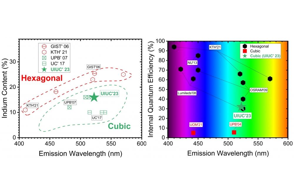
The state-of-the-art hexagonal (i.e., wurtzite) III-nitride green LEDs only reach half and one third of the wall-plug-efficiency goals of DOE in 2025 and 20235, respectively. The green gap can be solved using cubic (i.e., zincblende) III-nitride instead, as the advantages of cubic (In)GaN materials for SSL are well documented theoretically and experimentally. However, the actual efficiencies of cubic devices have been low due to the metastability of cubic GaN materials, hampering the quality and purity of cubic phase.
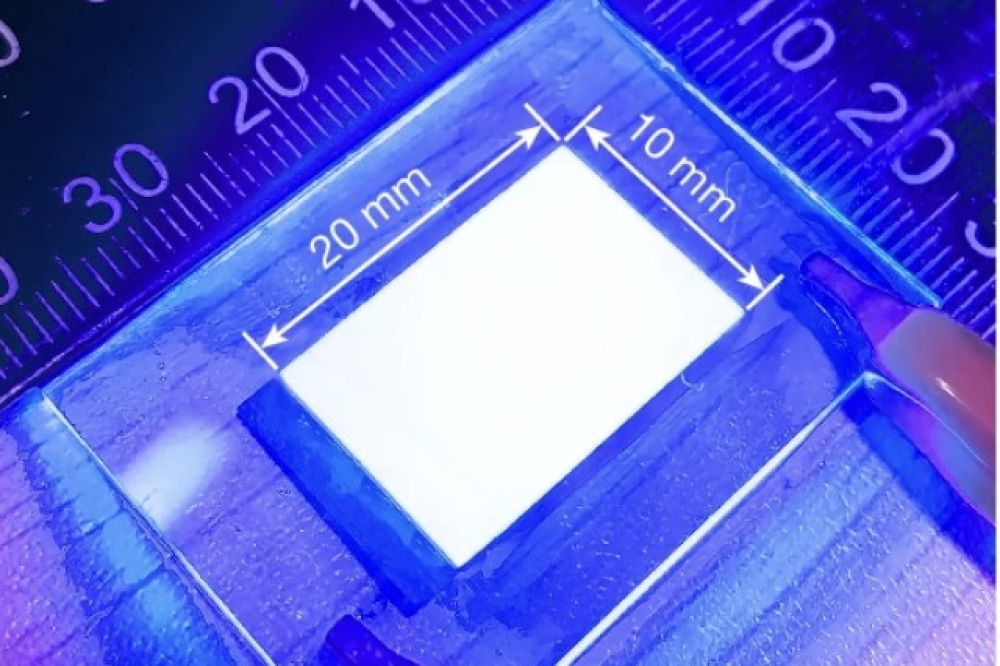
In Applied Physics Letters, Jaekwon Lee and Can Bayram at the University of Illinois report a green-emitting cubic III- nitride active layer with 32.0 ± 0.6 percent of internal quantum efficiency (IQE) and 16.0 ± 1.6 percent of indium content.
The Cubic GaN/In0.16Ga0.84N/GaN is more than six times higher efficiency than what is reported in the literature for conventional cubic active layers on 3C-SiC, and this has ~30 percent lower indium content than traditional hexagonal LEDs for green emission.
This demonstration is thanks to the aspect ratio phase trapping technique enabling high-quality pure cubic GaN top surface as well as a wide-quantum-well design specific to cubic III-nitrides.
Overall, the U of I team presents the highest efficiency green-emission from cubic III-N active layers that are at a comparable level with already-mature hexagonal active layers, promising for filling the green gap in solid-state lighting.
Reference
'Green-emitting Cubic GaN/In0.16Ga0.84N/GaN Quantum Well with 32 percent Internal Quantum Efficiency at Room Temperature' by J. Lee and C. Bayram,; Appl. Phys. Lett. 124, 011101 (2024)


