CEA-Leti to present papers on MicroLED progress
Photonics West papers will detail processing LEDs directly on 200 mm silicon substrates and minimising carrier-diffusion length
CEA-Leti will present two papers on its microLED technology advances at Photonics West 2024 about making matrices of LEDs with increased data-rate density, and strategies to reduce their efficiency loss at small sizes.
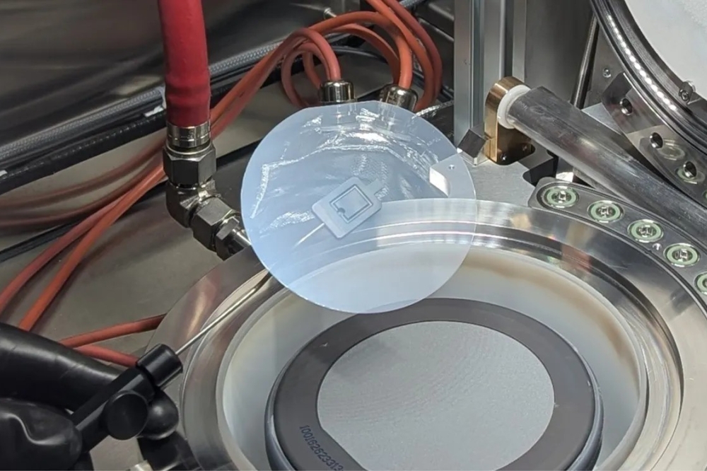
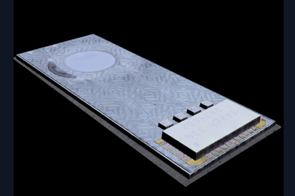
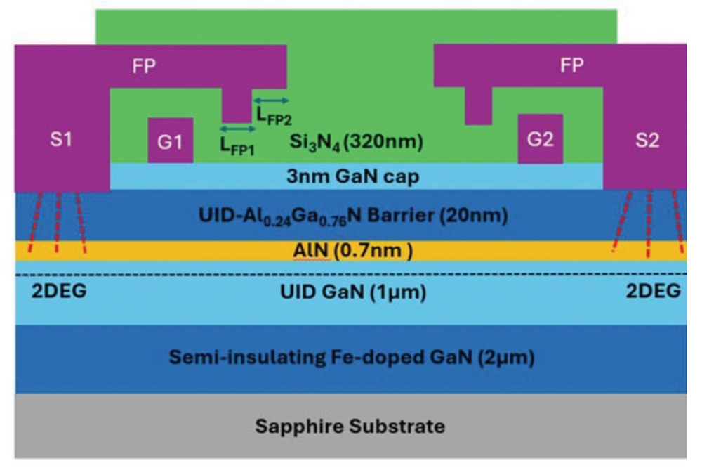
Described in the paper, 'Parallel Communication with InGaN/GaN Micro-LEDs Using a CMOS Compatible Approach', making LEDs directly on a 200 mm silicon substrate opens the way to producing a matrix of LEDs of a few microns that are individually controlled by dedicated CMOS circuits. (Jan. 31, 9:00 - 9:20 am PST, Moscone Center, San Fransisco, USA).
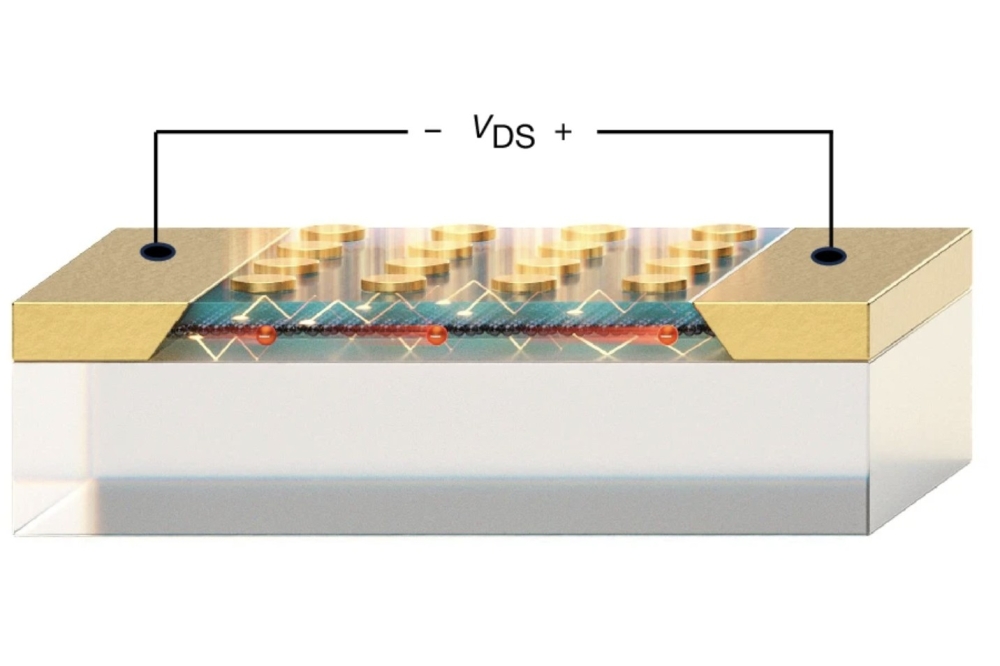
InGaN/GaN microLEDs are a strong candidate to enable high data-rate light communication because of their robustness, availability at large scale and ability to reach GHz scale bandwidth. Using them in an array enables massively parallel transmission leading to a high data-rate density. A CEA-Leti patented process to integrate a GaN LED matrix over a CMOS ASIC has also been developed. In this CMOS-compatible approach, the microLEDs’ integration was optimised by bonding them directly on top of a 200 mm silicon wafer and using GaN-based devices as both emitters and fast photodetectors.
“In order to address communication applications, we modulate LEDs at high frequency to reach a high data rate,” said Anthony Cibié, lead author of the paper. “Our aim is to use an array of LEDs to emit light and to detect it by an array of photodiodes, both made from GaN. We know how to fabricate thousands of pixels arrays, thus we can have thousands of parallel communication channels.”
Efficiency Improvement
Previous work has shown that microLEDs’ efficiency decreases as their size goes from the millimeter to micrometer range, because the number of carriers that can diffuse and recombine non-radiatively at defective sidewalls increases. Therefore, passivating the non-radiative centers and minimizing carrier-diffusion length appears to be critical to producing high-efficiency microLEDs.
For this reason, CEA-Leti has focused for many years on improving microLED efficiency, particularly by focusing first on defects passivation and more recently by understanding the impact of carrier diffusion, which is the subject of the second paper.
The second paper, 'Influence of quantum well thickness on carrier diffusion length in InGaN quantum wells grown on sapphire, freestanding GaN, and Si', highlights the strategy to reduce the InGaN/GaN LEDs’ efficiency drop that comes with smaller pixel size by understanding and controlling carrier diffusion. (Jan. 30, 9:20 PST, Moscone Center).
“In this presentation, we show experimentally that the diffusion length can be reduced by decreasing the thickness of the InGaN quantum well, as the theory predicts. In addition, we present a power-dependent, unexpected behavior of the diffusion observed in large quantum wells that may help us to understand the physics of the emitters,” said Simon Litschgi, lead author of the paper.
Litschgi noted that these phenomena were studied on several epitaxy substrates, including silicon. This paves the way to fabricating more efficient GaN microLED devices on 200 mm and 300 mm Si wafers, which is the most cost-effective industrial solution for display and communication applications.