Realising vertical deep-UV lasers
Deep-UV lasers with a vertical architecture have the potential to address issues associated with current injection
Engineers from Japan are claiming to have broken new ground with a deep-UV semiconductor laser with a geometry that’s vertical, rather than horizontal.
“This is an essential technology for increasing the optical output power in AlGaN-based deep-ultraviolet laser diodes,” remarks team spokesman Motoaki Iwaya from Meijo University.
According to Iwaya, a major downside of the majority of AlGaN-based devices, which are grown on semi-insulating materials such as sapphire and AlN to ensure a high crystal quality, is their lateral device geometry that limits current flow. This restriction in carrier transport stems from difficulties in p-type doping that hamper the realisation of large p-type electrodes with uniform current conduction.
To overcome this bottleneck, the team from Meijo University, Ushio and Seishin Trading are pursuing a vertical device architecture. This geometry has already demonstrated success in InGaN-based visible LEDs and laser diodes.
For AlGaN-based vertical devices, there’s a need to remove the insulating AlN or sapphire, a task that can be accomplished with either laser lift-off, electrochemical etching, or grinding and polishing.
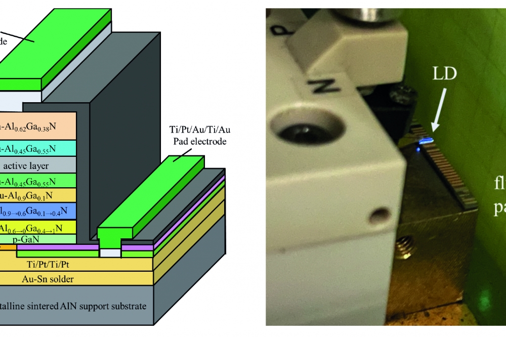
Iwaya and co-workers employ a form of exfoliation based on laser lift-off to extract material with a size of around 1 cm2. Efforts begin by growing the device structure on AlGaN templates with a foundation of AlN nanopillars that have been defined by nano-printing and inductively coupled plasma etching. This is an approach previously used by the team to fabricate AlGaN-based LEDs emitting in the UVB.
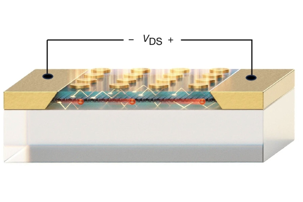
The laser structures are grown on 2-inch c-plane sapphire substrates with AlN nanopillars with a 400 nm terrace width that are 300 nm high and arranged in a triangular lattice pattern with a 1 mm pitch. On these pillars the engineers have used MOCVD to add a 5 mm-thick undoped Al0.68Ga0.32N template, a 170 nm-thick undoped Al0.5Ga0.5N layer designed for laser absorption in the lift-off process, and the device heterostructure (its details are provided in the figure).
Device fabrication continues with the cleaving of the epiwafer into 1 cm2 squares, the addition of polycrystalline sintered AlN for structural support – bonded to the heterostructure using a Au-Sn solder – and laser lift off with a pulsed laser emitting at 257 nm and providing an optical density of 0.53 J cm-2. Subsequent processing, including the addition of electrodes and scribing, creates lasers with cavity lengths between 500 nm and 1.2 mm.
Only around two-thirds of the lasers produced by the team have operated effectively, due to p-type electrode detachment. Iwaya and co-workers argue that yield loss comes from insufficient bonding strength with the support substrate, as well as substrate warpage during crystal growth and a sub-optimal selection of dielectric films and other components. Improving the selection of materials and processes should address these issues.
Using 50 ns pulses to drive lasers with a 1200 mm cavity length and a 5 μm aperture width produces an extremely sharp emission peak at 298.1 nm at a current density of 25 kA cm-2. At higher current densities, multiple lasing peaks are produced, with output power increasing to several milliwatts.
The introduction of additional peaks does not surprise Iwaya. “The optical cavity is designed without considering transverse and longitudinal optical confinement, so the laser is oscillating in multimode.” He says that modal confinement can be improved by adopting the cavity control techniques used for visible laser diodes.
One of the next goals for the team is to address the high operating voltage of the laser, which stems from the Schottky contact of the n-type electrode. “We aim to reduce the operating voltage by forming low-resistance ohmic n-type electrodes, and then to demonstrate the operation of a deep-ultraviolet laser diode with a watt-class optical output from a single chip by increasing the size of the device.”
Pictured above: The emission pattern of the 298 nm laser can be seen with phosphor-coated paper.
Reference
T. Nishibayashi et al. Appl. Phys Express 16 104001 (2023)