Building better multi-channel Schottky barrier diodes
Researchers from Singapore’s Nanyang Technological University and its Agency for Science, Technology and Research are claiming to have provided the first successful demonstration of functional devices using multi-channel AlN/GaN heterostructures.
“While other groups have reported impressive results for epiwafers, the critical challenge has been transitioning from material to working devices,” explains team spokesman, Hanchao Li, from Nanyang Technological University.
According to Li, a major breakthrough by their team has been the formation of stable ohmic contacts that avoid compromising the channel current in the Schottky barrier diodes. “This achievement is significant because the high aluminium composition and wide bandgap of aluminium nitride make ohmic contact formation particularly challenging in these heterostructures,” added Li.
Over the last few years, there has been much interest in multi-channel GaN devices. Their appeal is overcoming the limited current conduction of devices with a single channel, and ultimately circumventing the trade-off between sheet charge density and mobility.
A number of research groups have produced multi-channel devices by pairing GaN with either AlGaN or InAlN. However, the team from Singapore prefers the combination of AlN and GaN. This duo provides a higher polarisation-induced charge density, allows for excellent electrostatic control of the channel in the vertical direction when a thin AlN barrier is employed, and enables excellent carrier confinement within the channels.
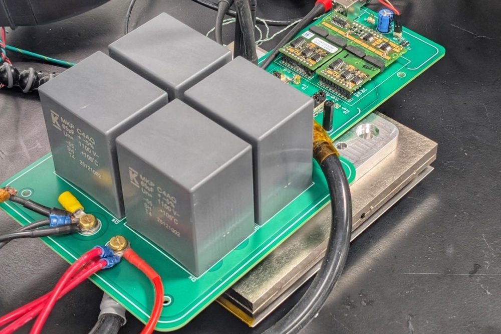
Fabrication of the team’s diodes has involved outsourcing epiwafer growth to a commercial MOCVD facility. The reasoning behind this decision is to ensure stability and reproducibility in epitaxial growth.
“Given that device performance is highly sensitive to material quality, consistent and reliable epitaxial layers are crucial for our device development and optimisation process,” argues Li.
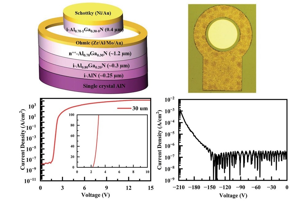
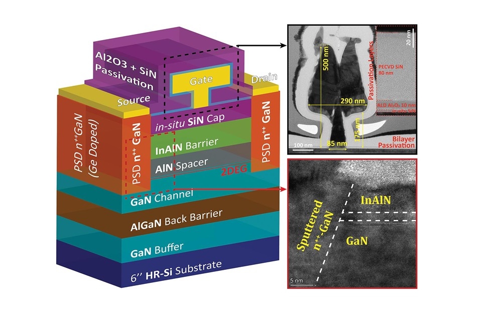
Characterisation of the team’s epiwafer, featuring five pairs of 4.9 nm-thick AlN barriers and 46.7 nm-thick GaN channels, reveals high-quality material growth. Scanning transmission electron uncovers sharp interfaces between the layers, and reciprocal space mapping produces well-defined, distinct peaks, indicating high-quality crystal growth.
To form diodes, Li and co-workers began by adding a cathode. To form this contact they applied an ohmic recess process, before adding Ti/Al/Ni/Au in this exposed region. The next step involved adding an anode, with this Schottky contact formed by plasma etching that enabled a direct sidewall contact between the two-dimensional electron gas and the anode. Post-anode annealing under nitrogen gas recovered nitrogen vacancies caused by the etching process.
Using the transmission line method, the team determined an optimal ohmic etching depth of 180 nm, corresponding to the mid-point of the fourth channel. Etching deeper, through all five channels, led to an increase in resistance, rising from the optimal value of 0.38 Ω mm to 0.64 Ω mm. The team attributes the higher value to the limited effectiveness of sidewall contacts.
Electrical measurements determined a turn-on voltage of just 0.5 V. For a diode with a lateral anode-to-cathode distance of 3 µm, 1.1 V produces a forward current of 100 mA mm-1, and current delivery can be as high as 1050 mA mm-1.
Operating under reverse bias, the breakdown voltage – defined as the voltage where the current exceeds a 1 mA mm-1 threshold – is 104 V, 268 V and 422 V for anode-to-cathode distances of 3 mm, 5 mm and 20 mm, respectively. These relatively low values are attributed to a combination of: an absence of electric field management structures, such as field plates and guard rinds, leading to a non-uniform electric field distribution and premature breakdown; and multiple cycles of AlN/GaN growth, which may introduce material quality issues that lead to increases in dislocation densities and interface states.
The team are now developing an approach for forming the ohmic contact that is based on the sputtering of GaN, and starting to investigate finFETs that are based on this epitaxial process. “We believe this could lead to enhanced device performance,” remarks Li.
Reference
H. Li et al. Appl. Phys. Express 18 016502 (2025)
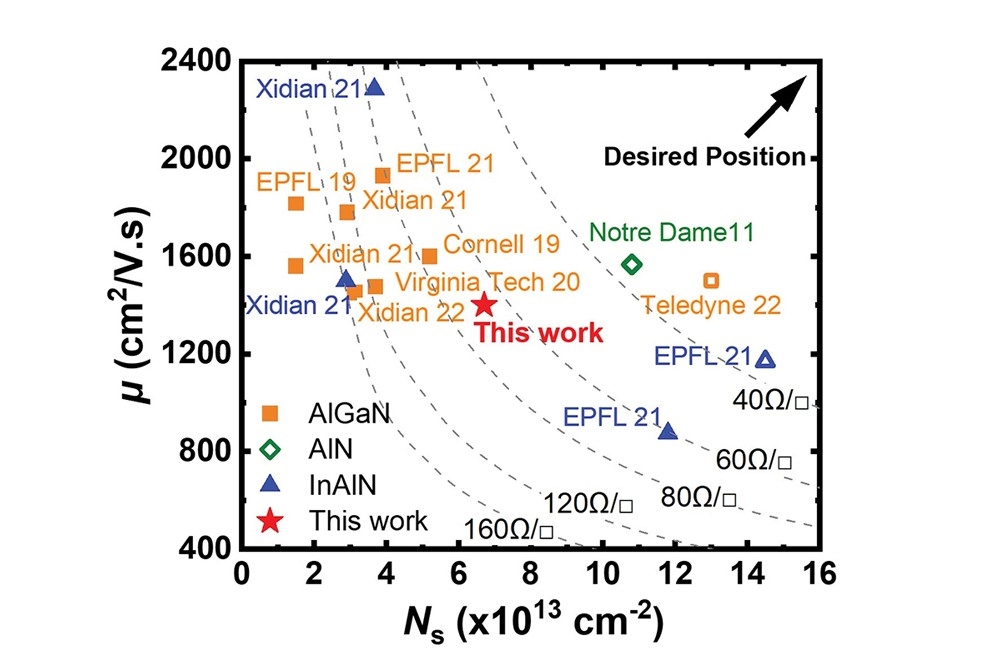
Pictured above: While the team from Singapore has not produced epiwafers with the very best combination of mobility and sheet charge density, they have produced the best device results. Note that the solid symbols are related to reports of fabricated devices on these heterostructures, while hollow symbols indicate otherwise.