Agnitron’s New Showerhead: Advancing MOCVD Technology
A novel showerhead featuring innovative gas injection accelerates MOCVD
growth while expanding the palette of epitaxial materials to include
AlScN.
BY AARON FINE, FIKADU ALEMA, WILL BRAND, VITALI SOUKHOVEEV, PAUL FABIANO AND ANDREI OSINSKY FROM AGNITRON
POWER ELECTRONICS is undergoing a transformation. Silicon is being replaced with the likes of GaN and SiC, members of a family of wide bandgap materials that are enabling devices to be smaller, more efficient and high-performing. But that’s just the beginning, with the focus shifting to the new frontier of ultra-wide bandgap materials, primarily AlN and Ga2O3.
Collectively, silicon’s superiors are grabbing an increasing share of the power device market, with total sales projected to to exceed $10 billion within just a few years. These high-performance alternatives are finding deployment in many sectors, including the military, electric vehicles, power supplies and photovoltaic inverters.
Playing a pivotal role within this dynamic landscape is our company, Agnitron Technology. We are developing and manufacturing an expanding portfolio of OEM semiconductor growth tools, including but not limited to MOCVD, CVD and HVPE technologies.
One of these three forms of deposition, MOCVD, is widely used for the manufacture of power electronics, as well as LEDs and lasers. This epitaxial growth technique, involving the deposition of substances onto a surface in a high-temperature chamber, ensures meticulous control of the film’s thickness, its composition, and its quality. These assets make MOCVD ideal for crafting high-performance layered structures in various devices.
It’s far from trivial to extend the use of MOCVD to the likes of AlN and Ga2O3, due to persistent hardware challenges. At Agnitron, we have recognised and started to address these specific challenges.

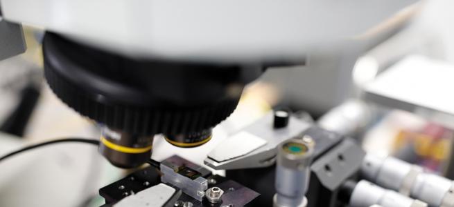
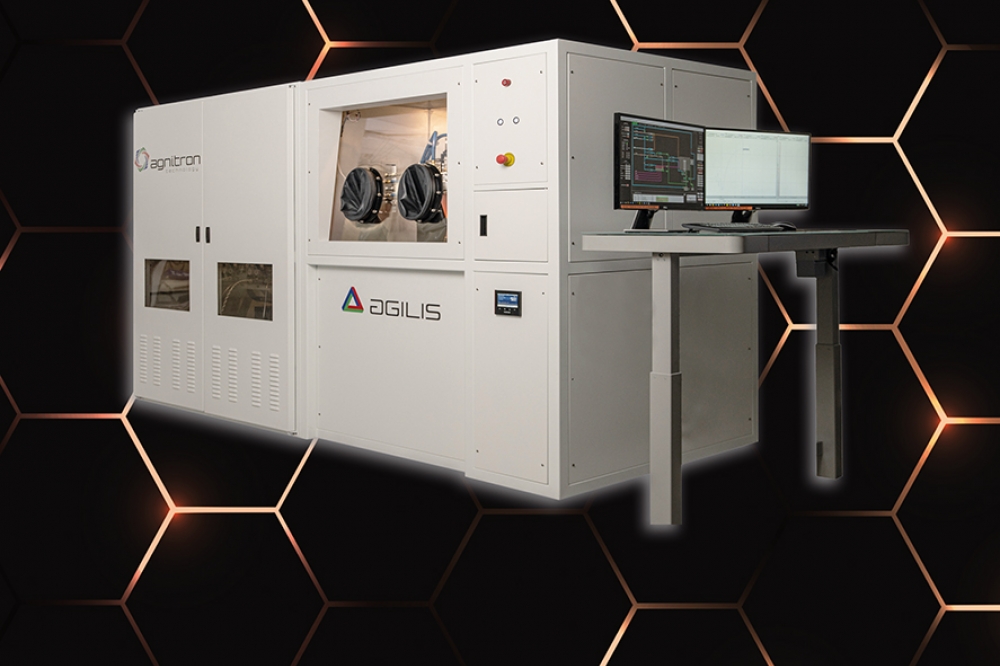
The Agnitron Agilis 100 features a Gen III Close Space Injection Showerhead, aiding the growth of an AlN film.
Gen III CIS
The biggest challenges in hardware design are associated with the showerheads, arguably the most crucial component for epitaxial semiconductor material growth. Traditional showerhead design focuses on facilitating multiple separate, consistent, uniform flows of temperature-regulated gases, by utilising various complex machining methods. Unfortunately, these designs result in expensive, fragile showerheads with a limited lifetime. Success has been held back by traditional manufacturing practices, which hamper efforts to realise faster growth rates, uniform film thickness and smooth surfaces – and the ability to grow films previously not possible with standard commercial MOCVD reactors.
Our team at Agnitron has broken through this impasse with an innovative, patent-pending showerhead technology that we incorporate into our vertical CIS Agilis reactors. Our triumph stems from advances in the initial design of the showerhead based on our previous Gen II CIS. When developing this particular reactor, which features a close injection showerhead (CIS), we focused on exploring a novel method for controlling the well-established hydride and alkyl delivery system. The immediate outcomes, soon discussed, showcase that this design provides precise control over thickness uniformity and surface roughness, as well as enhancing film growth rates and reducing the particle count on the wafer.
The new showerhead can be applied across different Agilis reactors, for the growth of materials such as GaN, AlN and AlGaN alloys, as well as for oxide-based materials, like Ga2O3 and AlGaO alloys. This innovative showerhead offers tremendous versatility, demonstrated by its ability to be heated to temperatures exceeding 150 °C that allow for the pre-heating of ammonia. This attribute also facilitates the growth of films utilising low vapor pressure precursors. An illustrative case is the growth of ternary and quaternary nitrides, including ScAlN, and YAlN, which have garnered a lot of interest recently for expanding the application possibilities of AlN.
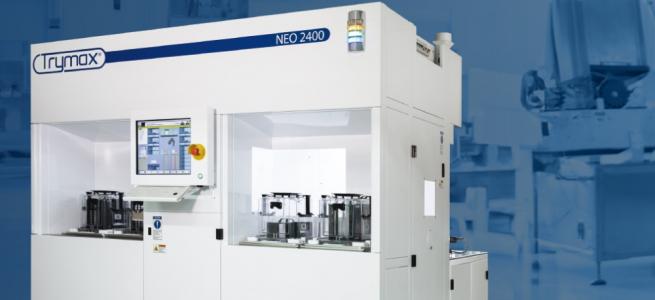
The Agnitron Agilis 100 MOCVD
One of our most prominent tools, the Agnitron’s Agilis 100 MOCVD, is recognised for its compact footprint and outstanding adaptability, and is capable of the growth of an incredibly wide variety of materials. Designed for R&D with smaller substrates but capable of accommodating larger wafers up to 100 mm in diameter, this tool can be used to grow: Ga2O3, AlN, AlGaN, GaN, InGaN, III-V As/P alloys, MgZnO, ZnO, II-IV compounds; transition metal dichalcogenides, such as MoS2, MoSe2, WS2, WSe2; phosphorene, two-dimensional hexagonal BN, SiC, ScAlN, and YAlN.
Offering enhanced usability, our Agnitron Agilis 100 integrates optical reflectometry in the UV and blue with Imperium analytical control software to provide real-time measurements of growth rate and thickness. Additionally, the Agilis 100 offers UV light exposure during growth, a feature that ensures effective control of epitaxial film purity by reducing residual carbon incorporation and managing point defects. Moreover, our Agilis 100, along with all our MOCVD/CVD systems, facilitates seamless plug-and-play switching between sources and gas distribution (showerhead) configurations – this is realised within just a few hours of maintenance. Another notable feature of the Agilis 100 is the option to add precursor distribution nozzles. This enables process refinement and wafer carrier cleaning, enhancing the appeal of these tools across a diverse range of applications.

Figure 1. Ga2O3 film growth in an Agilis 100 reactor with the
cutting-edge CIS showerhead. The growth rate (a) and uniformity (b)
dependencies on chamber pressure for TEGa and TMGa. Growth rate and
uniformity versus TMGa molar flow rate (c) for layers grown at substrate
temperatures of 800 °C and 900 °C and constant growth pressure of 30
Torr, achieving around 20 µm/hr at 540 µmol/min with less than 1
percent, 1σ uniformity.
There are two interchangeable configurations associated with the Agilis 100: the remote injection showerhead (RIS), and the CIS. The primary distinction is the placement of the showerhead relative to the wafer carrier. This ensures adaptable film growth options for meeting various research and development requirements.
Our RIS Agilis 100 reactor, capable of temperatures of over 1600 °C, features a distinctive remote injection showerhead that incorporates an optimised hydride or oxygen injector and uniformly distributes around it metalorganic precursors, such as trimethylgallium and trimethylaluminium. Commonly used for Ga2O3 growth, this configuration encounters two primary challenges. Firstly, film growth is impeded, due to higher gas-phase reactions, resulting from the increased gap between the showerhead and the wafer carrier. Secondly, it is harder to realise uniform film thickness and doping, due to difficulties in maintaining flow laminarity across the wider showerhead-to-wafer carrier gap.
Despite these limitations, our RIS Agilis 100 MOCVD reactor offers exceptional thickness uniformity within a tight process window. This is accomplished by lowering the reactor pressure and introducing high total gas flows to suppress buoyancy, which threatens to lead to flow instabilities. However, while the RIS Agilis 100 enables uniformity below 2 percent across a 50 mm substrate, process efficiency falls, due to high gas and precursor consumption, coupled with the narrow process window.
As mentioned earlier, the challenges just discussed can be addressed by equipping the Agilis 100 with the new Gen III CIS showerhead. Note that this is available as an upgrade. We have conducted extensive testing of our Agnitron Agilis 100 reactor for Ga2O3 growth, with evaluation showcasing the enhanced performance that comes from introducing the new showerhead. This design overcomes the limitations associated with the RIS configuration.

Figure 2. Ga2O3 two-dimensional thickness map on a 50 mm sapphire
substrate using the CIS. Films grown at 1.6 µm/hr(a) and 20 µm/hr (b).
Uniformity remains below 1 percent for both growth rates. A 2 mm edge
exclusion has been applied during the thickness map.
Agnitron and Ga2O3
One of the primary applications for our new Gen III CIS showerhead is the growth of epitaxial layers of β-Ga2O3, a pivotal material for advancing power device technology. Positioned to shape the future of the power semiconductor market, Ga2O3 possesses fundamental properties that are conducive to the production of superior power devices while maintaining economic viability through the creation of high-quality melt-grown bulk substrates.
Over a decade of dedicated research in device and materials, Ga2O3 has demonstrated remarkable progress. Breakthroughs at the device level include a breakdown voltage now exceeding 8 kV and critical breakdown fields of more than 5 MV cm-1, surpassing the theoretical limits of SiC and GaN. Such success has established β-Ga2O3 as the most promising candidate for next-generation solid-state power-switching applications.
A critical process in the production of any material is the growth of the epitaxial layers. With β-Ga2O3 films, epitaxy has been extensively explored with various methods. Of these growth technologies, MOCVD stands out for its ability to produce high-quality epitaxial films at a rapid growth rate, ensuring uniformity and controllable doping.
Our team at Agnitron Technology is leading many of the breakthroughs in Ga2O3 materials – they are spearheaded by the design and building of customised MOCVD reactors and processes for growing high-purity films of this oxide and its related alloys.
Our renowned Agnitron Agilis MOCVD reactors are widely adopted worldwide, utilised in prestigious institutions that include but are not limited to: the University of California, Santa Barbara (UCSB); Cornell University; US Naval Research Laboratory (NRL); the Ohio State University; Arizona State University; the University of Wisconsin; and Bristol University, UK. Our reactors are being used by research teams at these institutions, with these epitaxial tools behind the growth of high-purity Ga2O3 films, including those with impressive electron mobilities of nearly 200 cm2 V-1 s-1 at room temperature and over 23,000 cm2 V-1 s-1 at low temperatures. Noteworthy results, underpinned by growth using our Agnitron reactors, have featured in previous issues of CS Magazine – see issues 2 and 7 of 2022, and issue 3 and 6 of 2023.

Figure 3. (a) Growth rate as a function of TMAl molar flow rate. The
inset in (a) shows the growth rate as a function of substrate
temperature. X-ray rocking curves, obtained with 2.4 µm-thick AlN, show
values for the full-width at half maximum of 280 arcsecs (002) (b) and
354 arcsecs (102) (c).
The availability of native Ga2O3 substrates, reaching sizes of up to 100 mm in diameter, presents a significant opportunity for commercialising β-Ga2O3-based power devices. However, as is often the case with epitaxy, the primary challenge lies in attaining precise thickness and doping uniformity, along with a consistently smooth surface, all while maintaining an industrially feasible growth rate. Our ground breaking Agnitron Gen III CIS showerhead tackles this challenge, offering a solution to elevate film quality. This advance is a critical step towards enhancing film manufacturability, and ultimately positioning β-Ga2O3-based power devices for market success.
Gen III CIS: Growing Ga2O3
We incorporated the Gen III CIS showerhead into our Agnitron Agilis 100 reactor for the growth of Ga2O3. The results accentuate the showerhead’s effectiveness in enhancing growth rates and producing exceptional thickness uniformity (see Figure 1 and 2). Using a substrate temperature of 800 °C, we studied the influence of chamber pressure on the growth rate of films produced using two different gallium-based precursors: trimethylgallium (TMGa) and triethylgallium (TEGa). When investigating the influence of chamber pressure, we adopted consistent molar flow rates of 46 µmol min-1 for TEGa and 25 µmol min-1 for TMGa.
At elevated growth pressures, the growth rate falls for both TEGa and TMGa, due to unintended gas-phase reactions. These reactions deplete the precursor before it reaches the substrate, thereby reducing the necessary substrate surface reactions for film growth.
Despite TEGa having a higher molar flow rate, it is the films grown with TMGa that have a higher growth rate, highlighting the efficiency of the TMGa source. The accelerated growth kinetics of TMGa compared with TEGa stem from a pyrolysis process that involves two steps, rather than three. This enables TMGa to react more rapidly with oxidising gases and have a higher growth rate.

Figure 4. (a) Thickness map for a 0.73 µm-thick AlN film and (b) an
atomic force microscopy image of a 2 µm-thick AlN layer on a sapphire
substrate. Notably, these films showcase exceptional smoothness, with a
uniformity of less than 0.33 percent.
Compared with TEGa, the influence of growth pressure on films grown with TMGa is less pronounced, indicating reduced impact of gas-phase reactions for films grown with this precursor. The uniformity of films grown with TMGa is notably superior, consistently measuring below 1 percent, while for TEGa it is below 2.5 percent.
We have also studied the impact of flow rate on the Ga2O3 growth rate. For TMGa it’s a linear relationship, with the growth rate reaching approximately 20 µm/hr for a TMGa flow of 540 µmol/min (see Figure 1 (c)).
To evaluate film uniformity under different growth rates with TMGa, we produced thickness maps for two films (see Figure 2). These maps highlight the new showerhead’s capacity to produce films with less than 1 percent non-uniformity, irrespective of growth rate.
Another encouraging result is that using silane as a dopant, Ga2O3 films grown at 4.3 µm/hr with TMGa exhibit an electron mobility of 100 cm2 V-1 s-1 and a free carrier concentration of 4.6 x 1017 cm-3. This set of results confirms the new showerhead’s ability to produce high-quality Ga2O3 films.

Figure 5. Rutherford backscattering spectroscopy of ScAlN alloys grown
on GaN-on-sapphire templates using Agnitron’s Agilis 100. The blue trace
shows around 9 percent scandium, while the black trace shows 24 percent.
Gen III CIS: Growing AlN
The significance of AlN cannot be overstated. Blessed with remarkable properties, it is a superb candidate for next-generation high-power electronic and optoelectronic devices. Boasting a substantial bandgap of 6.1 eV, Schottky barriers exceeding 2 eV, an excellent thermal conductivity of more than 150 W m-1 K-1, and critical breakdown fields surpassing 15 MV/cm, AlN holds promise across various applications. To harness its full potential, high-temperature growth by MOCVD is employed, with temperatures exceeding 1300 °C to ensure a low defect density in the epilayers. Ideal for this task is the Agnitron Gen III CIS. Offering exceptional thermal control capabilities, it stands out by easily withstanding temperatures of over 1350 °C, and operating in close proximity to the susceptor, thanks to its new highly efficient thermal management.
Utilising our innovative CIS showerhead, we’ve conducted extensive tests, growing AlN on 50 mm c-plane sapphire substrates. Our results underscore our showerhead’s versatility, allowing for adjustable aluminium molar flow rates and, consequently, demonstrating impressive film growth rates, ranging from 0.7 µm/hr to around 9 µm/hr (see Figure 3(a)).

Figure 6. A 0.15 µm-thick film of ScAlN grown on GaN-on-sapphire.
We have explored the growth rate’s dependence on substrate temperature, finding a less pronounced effect. However, as substrate temperature increases, the gradual decline in growth rate is evident, a parameter we plan to investigate in more detail. Notably, our Agnitron Gen III CIS allows fine tuning of the distance between the showerhead and the wafer – it can be below 10 mm, and more than 35 mm. This tremendous versatility facilitates diverse precursor allocations and growth scenarios, enhancing the showerhead’s adaptability to varied experimental conditions.
Using our novel CIS showerhead reactor, we have grown a 2.4 µm-thick AlN layer on sapphire substrates at a growth rate of around 1.0 µm/hr. X-ray diffraction indicates excellent crystal quality, with values for the full-width at half maximum of the diffraction peak of around 280 arcsecs and 350 arcsecs in the (002) and (102) directions, respectively (see Figure 3(b) and 3(c)). Note that these results are obtained without optimisation of the process conditions. These AlN thin films have a remarkable thickness uniformity and minimal surface roughness, with a uniformity of less than 0.5 percent for a AlN film that’s around 0.7 µm thick, grown at about 0.7 µm/hr (see Figure 4(a)). Outstanding smoothness is evidenced by a root-mean-square roughness of just 0.145 nm for a AlN-on-sapphire film that’s 2 µm-thick, and grown at 1.3 µm/hr (see Figure 4(b)). These findings underscore the efficacy of our new showerhead in producing high-quality AlN films at a high growth rate that exhibit impressive uniformity and surface characteristics.
Why ScAlN?
High-performance microwave transistors and amplifiers are vital for wireless communication, with GaN-based HEMTs playing a key role. AlGaN serves as a common barrier material, forming a two-dimensional electron gas at the AlGaN/GaN interface. However, the critical thickness of AlN/GaN is insufficient for forming a Schottky gate contact, resulting in devices with high leakage. Emerging as a promising barrier layer is the alloy scandium aluminium nitride (ScAlN). Due to its high polarisation coefficients, its shows superiority over standard AlGaN barriers.
MOCVD is a promising growth technology for the growth of ScAlN on an industrial scale, as there is the potential to produce high-quality, uniform films on large wafers. However, to date, only the group at Fraunhofer IAF, in Freiburg, Germany, has demonstrated the growth of ScAlN by MOCVD. To address this shortcoming and help unleash the substantial market potential for the ScAlN material system, we have been developing a commercial-scale MOCVD process for ScAlN/GaN HEMTs.
Holding back the growth of ScAlN with existing commercial MOCVD reactors is the lack of scandium-based metal-organic precursors with a sufficiently high vapour pressure. The vapour pressure of these particular precursors is very low, and the introduction of a sufficient flux into the reactor chamber requires heating the sources to a relatively high temperature. That’s far from trivial, as it demands that all the gas delivery components – including the mass flow controllers, pressure controllers and valves – sustain an even higher temperature to prevent precursor condensation in the delivery network. This necessitates the use of specialised components and assemblies that are capable of withstanding these far high temperatures. Current commercial MOCVD reactors are not designed to deliver such low-vapour-pressure precursors, as they are commonly built to handle the traditional metal organics, which have sufficiently high vapour pressure, even at room temperature.

Figure 7. Composition of a ScAlN film measured by Rutherford
backscattering spectroscopy across the diameter of a 50 mm wafer. The
average composition and coefficient of variation are 7 percent and 4.8
percent, respectively.
We have addressed the challenge of gas delivery of scandium-based sources by developing and implementing a specialised high-temperature gas delivery system. We heat the source to 150 °C, and maintain the gas delivery network near 200 °C. By integrating this system with our Agnitron Agilis 100 reactor, we have developed the growth processes for producing high-quality ScAlN thin films on wafers up to 50 mm in diameter using commercially available scandium sources. Our ScAlN alloys have scandium compositions that can exceed 40 percent, despite an unoptimised process.
To evaluate the absorption band edge shift and the crystal quality of our ScAlN films, we have turned to optical transmission and X-ray diffraction. These techniques consistently demonstrate the successful incorporation of scandium into the AlN lattice while preserving the wurtzite structure. We meticulously control scandium integration by adjusting the source temperature, reactor pressure, substrate temperature and ammonia flow rate. For accurate determination of the scandium composition in our ScAlN thin films, we utilise both energy-dispersive X-ray spectroscopy and Rutherford backscattering spectroscopy. The results from both techniques are in good agreement (see Figure 5 for Rutherford backscattering spectroscopy results, highlighting peaks for scandium, aluminium and gallium in four films).
Introducing our Gen III showerhead for ScAlN growth delivers a remarkable performance. Consistently, it is capable of producing highly uniform ScAlN films with a thickness uniformity of less than 1 percent. We investigated the scandium compositional uniformity of these films with Rutherford backscattering spectroscopy (see Figure 6). The measurements reveal a uniform scandium content across the entire wafer: the average scandium composition is 7 percent, and the variation is 4.8 percent of the mean value (see Figure 7). These preliminary results show a promising compositional uniformity, and we expect further improvement following the manipulation of showerhead temperature and process flowrates. The root-mean-square (RMS )surface roughness of a ScAlN/AlN/GaN HEMT structure, grown on SiC substrate, is just 0.2 nm (see Figure 8). In the non optimized ScAlN/GaN HEMT structure sheet carrier concentration was measured 1.9 x 1013 cm-2 and electron mobility about 900 cm2 V-1 s-1.
Success with ScAlN opens the door to the growth of a number of technologically significant nitride materials that have to be grown with low-vapour pressure precursors. They include transition metal nitrides, such as NbN and YAlN.
The results just presented highlight our Agnitron Gen III CIS’s remarkable ability to surpass the thickness, doping, and composition uniformity requirements that are essential in production MOCVD, all while maintaining a high growth rate. As well as demonstrating state-of-the-art devices, this new capability offers a cost-effective solution for researchers using MOCVD to make radical breakthroughs in power electronics.

Figure 8. A 2 µm by 2 µm scan of a ScAlN/GaN HEMT structure grown on SiC. The root-mean-square (RMS) roughness is 0.20 nm.
Innovation pedigree
Standing at the forefront of semiconductor innovation, our team at Agnitron Technology is revolutionising the growth of wide and ultra-wide bandgap materials with our ever-advancing portfolio of cutting-edge MOCVD tools. Our focus on overcoming longstanding challenges in showerhead design has spurred the introduction of the Gen III CIS showerhead, showcased in the Agilis 100 reactor. The results obtained with this tool are transformative, enabling us to demonstrate enhanced growth rates, improvements to thickness and alloy composition uniformity, and a film quality exceeding production MOCVD standards. Success on all these fronts comes while maintaining a high growth rate. As well as delivering exceptional performance, the Agnitron Agilis 100 MOCVD system stands out from the crowd for its adaptability and seamless configuration changes. This tremendous versatility enables a spectrum of epitaxial growths, allowing users to explore any imagined possibilities.
As we continue to push the boundaries of materials growth, our tools and growth technologies are paving the way for advancements in power electronics, while solidifying our position as a leader in the semiconductor research equipment manufacturing industry. Our belief is that by focusing on such innovation, we will bolster the future viability of our customers to bring their products to market faster, more reliably, with higher quality and thus make a more meaningful contribution to society at large.
•Agnitron would like to acknowledge Greg Haugstad of the University of Minnesota Characterization Facility (UMN CharFac) for conducting RBS measurements and Prof. Chirag Gupta of the University of Wisconsin Madison for XRD measurements.
Further reading
F. Alema et al. “Fast growth rate of epitaxial β–Ga2O3 by close coupled showerhead MOCVD” J. Cryst. Growth 475 77 (2017)
G. Seryogin et al. “MOCVD growth of high purity Ga2O3 epitaxial films using trimethylgallium precursor” Appl. Phys. Lett.117 262101 (2020)
Y. Zhang et al. “MOCVD grown epitaxial β–Ga2O3 thin film with an electron mobility of 176 cm2/V s at room temperature”, APL Mater. 7 022506 (2019)
M. Baldini et al. “Semiconducting Sn-doped β–Ga2O3 homoepitaxial layers grown by metal organic vapour-phase epitaxy” J. Mater. Sci. 51 3650 (2015)
S. Manna et al. “Tuning the piezoelectric and mechanical properties of the AlN system via alloying with YN and BN” J. Appl. Phys. 122 105101 (2017)
S. Leone et al. “Metal-Organic Chemical Vapor Deposition of Aluminum Scandium Nitride” Phys. Status Solidi RRL 14 1900535 (2020)