SiC MOSFETs: Scrutinising the gate atom by atom
BY LAKSHMI KANTA BERA, SHIV. KUMAR, NAVAB SINGH, UMESH CHAND, ABDUL HANNAN BIN IBRAHIM ABDULLAH YEO, VOO QIN GUI ROTH AND SURASIT. CHUNG FROM A*STAR AND PIERRE-YVES CORRE FROM CAMECA INSTRUMENTS
OVER THE LAST DECADE, much effort has been devoted to the development of the SiC MOSFET. This is paying off, with sales soaring, driven by the uptake of this device in electric vehicles.
The success of the SiC MOSFET comes from its key attributes. One great strength is its wide bandgap, enabling high-temperature operation and a trimming of energy loss during device operation. Additional assets include its high thermal conductivity, aiding efficient heat dissipation and helping maintain device performance and longevity; and a simple integration flow, following in the footsteps of silicon technology, that involves the growth of SiO2, using thermal oxidation.
However, the SiC MOSFET has an Achilles heel. In stark contrast to the interface of silicon and its native oxide, SiO2, that grown on SiC is riddled with a high interface-state density. The numerous imperfections significantly reduce carrier mobility in the MOS channel and threaten device reliability.
Due to these significant concerns, much effort has been devoted to understanding the origins of the high density of interface states. This has been attributed to carbon-related defects, including C-clustered, C-interstitial, and C-vacancies. Within the scientific community, it is widely agreed that these defects play a significant role in influencing the density of interface states at the SiC/SiO2 interface.
Many studies, such as those investigating native point defects and carbon clusters in 4H-SiC, as well as the structure and energetics of carbon-related defects in SiC, have provided much insight into the impact of these carbon-related defects on material properties. However, despite many years of investigation by several research groups, the distribution of different elements and compounds in bulk SiO2 and at the SiO2/SiC interface is yet to be completely understood. To a large extent, this comes down to a lack of information at the atomic scale. There is a need to know the identity and the precise location of different species.
Two common techniques for materials characterisation that fall short in this regard are X-ray photoelectron spectroscopy and Auger electron spectroscopy. Both these forms of spectroscopy are hampered by a poor lateral resolution in the micrometre-range, as well as a relatively poor detection limit – it is around 0.1 atomic percent – that leads to a low detection sensitivity, and hampers complex quantification of chemical analysis.
Another widely used technique within the compound semiconductor community, secondary ion mass spectrometry, excels in detecting trace elements down to parts-per-billion levels. However, its sub-micrometre lateral resolution limits atomic-scale analysis. In addition, quantification of results is challenging, due to the dependency on ionization energy for secondary ion yield.
A versatile tool that provides detailed investigations at the sub-nanometre level is high-resolution transmission electron microscopy. Advances in one form of this, high-angle annular dark-field scanning transmission electron microscopy, have enabled, in special cases, three-dimensional characterisation at the atomic scale.
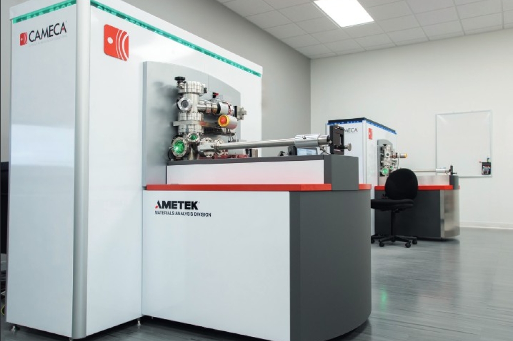
However, the ultimate characterisation technique for studying materials at the atomic level is atom probe tomography. This incredibly powerful technique, which our team from the Agency for Science, Technology and Research, Singapore, is using to scrutinise the interfaces of SiO2 and SiC, can’t be beaten when it comes to discovering the position of individual atoms in materials with nearly atomic resolution. One of its key merits is equal sensitivity for all elements.

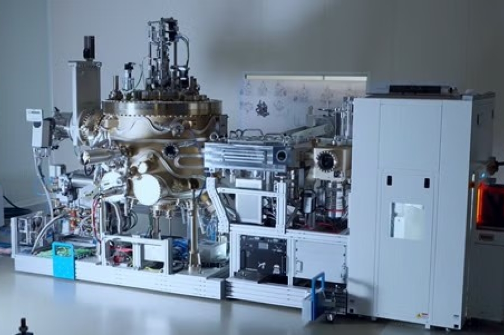
Figure 1. The experimental setup for atom probe tomography.
Basic principles
Atom probe tomography operates on the principle of field evaporation, with surface atoms extracted from specimens with an electric field. This process involves directing a laser at the sample, alongside simultaneous high-voltage pulsing, conditions that cause surface atoms to evaporate with near 100 percent ionisation. The evaporated atoms are projected onto a position-sensitive detector for analysis.
To maximise the effectiveness of this technique, there is a need to prepare sharp needle-shaped specimens with a radius of 50-100 nm. Such samples ensure precise analysis through field evaporation of surface atoms. The chemical nature of the atoms is identified with time-of-flight mass spectrometry (see Figure 1 for an overview of this experimental setup).
After loading samples into an atom probe tomography analysis chamber, specimens are cooled to around 50 K and maintained in an ultra-high vacuum, typically 10-11 Torr. Applying a DC voltage of typically between 2 kV and 10 kV results in a high electric field at the surface of the tip. The field at the tip’s apex is proportional to the applied voltage, and inversely proportional to its radius of curvature.
For electrically conductive materials, atom probe tomography involves the application of voltage pulses to the tip to generate an electrical field that induces field ionization. For less conductive samples a different approach is needed, with laser pulses ensuring the thermal evaporation of ions. The application of laser pulsing is especially advantageous in higher resistivity materials, such as semiconductors, where high-voltage pulses alone may be insufficient for promoting field ionisation.

Figure 2. Schematic cross section of sample for interest of investigation of several elements and their distributions.
The detection of ions that are liberated from the sample is correlated to the high-voltage and laser pulses. Ions are converted into a mass-to-charge-state ratio, measured in a unit known as the Dalton. This conversion is crucial for chemical identification of each ion, which is identified by the relationship between its time-of-flight and its mass-to-charge-state ratio.
A mass spectrum is produced during atom probe tomography – this is a histogram of the resulting mass-to-charge ratio of the detected ions. The correlation of the chemical and physical properties of a specimen’s surface aids characterisation of the mass spectra, as well as improving the precise accuracy of compositional material analysis and initial position at the specimen surface.
To determine the spatial distribution of atoms at the atomic scale, there is a need to generate a three-dimensional reconstruction of the analysed volume. This enables the determination of the local chemical composition of any arbitrary sub-volumes with a sub-nanometric resolution. Note that metals can provide concentration profiles with a depth resolution better than half an atomic plane.
Studying SiC MOSFETs
Within the SiC community, a two-step oxide-formation process has been widely adopted for making power MOSFETs. This involves either the thermal oxidation of SiC; or deposition of SiO2, followed by interface nitridation with a nitric oxide gas. Neither process is ideal, leading to a high density of interface states. This issue continues to motivate effort to consider other processes for forming the gate oxide.
We have used atom probe tomography to study SiC MOSFETs produced with alternative processes that have much promise. Our study has considered both pre- and post-oxidation treatment with and without hydrogen gas, and the impact of a post-oxidation anneal using nitric oxide.

Figure 3. Typical scanning tunnelling electron microscopy images of a sample ready for atom probe tomography measurements.
Our interest lies in understanding the elemental distribution of silicon, oxygen, carbon, nitrogen, hydrogen and argon in SiO2, the SiO2/SiC interface, and SiC beneath the SiO2 layer (see Figure 2 for an illustration of the cross section of different zones of the sample). Through the use of atom probe tomography, we are able to gain insight into the composition and structure of these materials, and ultimately enhance our understanding of device characteristics, including interfacial properties, reliability of the gate oxide and MOSFETs channel mobility. In turn, these findings can enhance the development of new technologies and materials with improved performance and functionality.
The preparation of our sample began by sputtering 100 nm of nickel, followed by 300 nm of platinum, on the oxide surface to prevent subsequent damage. We then used annular ion beam milling at 30 kV to produce a needle geometry with a tip diameter of no more than 100 nm (see Figures 3(a-d) for typical images of the prepared sample).
To mitigate damage from gallium implantation during the focused-ion beam process used for milling, all our specimens underwent low-energy cleaning with a 1 kV ion beam. This step is crucial for maintaining sample integrity and ensuring accurate results.
Our atom probe tomography measurements were undertaken with a laser power of 0.10 nJ/pulse to elucidate the influence of hydrogen gas treatment on the SiO2/SiC interface. To ensure data reliability, we repeated experiments three times, for each type of sample. This ensured a rigorous approach, which gathered consistent, replicable results (see Table 1 for experimental details).
Atom probe tomography has enabled us to investigate the impact of hydrogen gas treatment before oxidation and after oxidation on the atomic distribution of different species in SiO2 and at the SiO2/SiC interface. Those species include carbon, nitrogen, oxygen, silicon and hydrogen (see Figure 4 for the line scan mass spectrum of different species and the three-dimensional elemental distributions for our sample that involved pre-oxidation hydrogen gas treatment, oxygen gas oxidation, and nitric oxide post-oxidation annealing).
The primary providers of the nitrogen signal are normally 7 Da (N++), 14 Da (N+), and 28 Da (N2+). Of these three, the detection of a possible N+ signal at 14 Da is obstructed by the large Si++ signal.

Table 1. Experimental parameters used for atom probe tomography analyses.
For naturally abundant silicon, the ratio between Si-28/29 is 19.7. That’s not the case for our sample with pre-oxidation hydrogen gas treatment, oxygen gas oxidation, and nitric oxide post-oxidation annealing. The presence of nitrogen at the interface changes this ratio, which is higher than that expected by a factor of 2.4. Using this piece of information, we applied a correction to deconvolute the nitrogen signal at the interface, obtaining an accurate concentration for this element of 4.0 percent. The three-dimensional atomic distribution clearly shows significant nitrogen incorporation, predominantly at the SiO2/SiC interface, with some traces in bulk SiO2 as observed from the N2+ distribution map. Carbon is absent in both the SiO2 and SiO2/SiC interface.
We have also investigated the region-specific mass spectra of the SiO2/SiC interface of the MOSFETs that undergo oxidation with oxygen gas, and post oxidation annealing under hydrogen gas and then nitric oxide. Region-specific mass spectra of the SiO2/SiC interface are shown in Figure 5. There are a large number of nitrogen-containing peaks in this data, with red arrows used to indicate nitrogen-containing signals at the interface region.

Figure 4. The mass spectrum containing the interfacial region between
SiO2 and SiC from W4 obtained using atom probe tomography. Enrichment of
nitrogen at the SiO2/SiC interface is clearly observed in
three-dimensional distribution maps.
The ejection of complex ions from this sample, a situation not observed in the other sample, suggests that the combination of post-oxidation annealing under hydrogen gas and then nitric oxide treatment at high temperatures may lead to the production of many compounds through a complex process. This process involves diffusion of hydrogen gas and nitric oxide, as well as a chemical reaction involving various atoms, including silicon, carbon, nitrogen, oxygen, and hydrogen.
On the other hand, the sample that has undergone hydrogen gas treatment before oxidation may have potentially taken part in hydrogen-termination, diffusion into interstitial spaces, and the creation of carbon-hydrogen bonds. Subsequent oxidation of the SiC surface layer may have decreased the possibility of a chemical reaction that forms many complicated compounds during post-oxidation annealing by nitric oxide.

Figure 5. Distribution of nitrogen-related signals in the analysed
volumes obtained by atom probe tomography for the SiO2/SiC interface
subjected to oxidation with oxygen gas, and post oxidation annealing
under hydrogen gas and then nitric oxide. Peak assignment has been
undertaken based on the m/Z values: 7Da for N++, 27Da for SiCN2+, 28Da
for Si+ and N2±, 35Da for Si2N2+, 42Da for N3+, and 52Da for N2C2 +,
respectively.
We are surprised to note that our atomic concentration profiles show that there is nitrogen enrichment, confined at the interface to a depth of around 2.8 nm. We also note that we find no evidence for excess carbon or clustering in the bulk oxide, at the interface, or in SiC beneath the interface. Examining the hydrogen gas species, we observe an increase in the hydrogen signal in SiO2 with depth, spikes at the SiO2/SiC interface, and then a sharp decrease after crossing the interface.

The 2.8 nm-thick interfacial layer, rich in nitrogen and hydrogen, acts as a transition layer between materials. The presence of nitrogen and hydrogen plays a crucial role in reducing carbon cluster formation and passivating carbon or silicon-related defects at the interface. This passivation process helps to trim the interface state density and thus enhance the performance of the MOSFET, including its reliability. Further investigation is essential to verify both channel mobility enhancement and reliability properties of SiC power MOSFETs.
•This work was supported by A*STAR (Agency for Science, Technology and Research Singapore) under Grant No. A20H9A0242.