Research Review: Our ten top stories from the last thirty years
Exposing indium clustering
How can GaN LEDs be so efficient, despite being riddled with defects? One potential answer, attracting much attention in the device’s early days, is that defect-free indium clusters in the InGaN quantum wells localise carriers and ensure efficient recombination. But subsequent work by Sir Colin Humphreys’ team at the University of Cambridge poured cold water on this idea, indicating that clustering was a measurement artefact, caused by the electron beam. Irrefutable proof followed in 2011, when researchers at Cambridge and Oxford studied two samples with InGaN quantum wells, with one previously irradiated with an electron beam. Using atom probe tomography, this partnership found that the exposed sample had compositional inhomogeneities in its indium content. In comparison, the control sample had a naturally occurring, random distribution of indium atoms. S. Bennett et al. Appl. Phys. Lett 99 021906 (2011)
DEBUNKING A DUBIOUS ASSUMPTION
When determining the internal quantum efficiency of a device’s active region, researchers tend to assumme that this efficiency will equal 100 percent at very low temperatures. But this approach is flawed, according to investigations by Cam Bayram and co-workers from the University of Illinois at Urbana-Champaign. To obtain accurate values for the internal quantum efficiency of light-emitting structures, they don’t advocate any alternations to the starting point, the acquisition of photoluminescence spectra at a wide range of sample temperatures. But they argue that as well as looking at the prominent photoluminescence peak, it’s crucial to consider defect luminescence behaviour and thermal quenching. Putting their ideas into practice, this team has obtained values for the internal quantum efficiency of LEDs grown on silicon and sapphire, using modelling and values of photoluminescence intensity from a number of peaks. Y. Chiu et al. Appl. Phys. Lett. 122 091101 (2023)
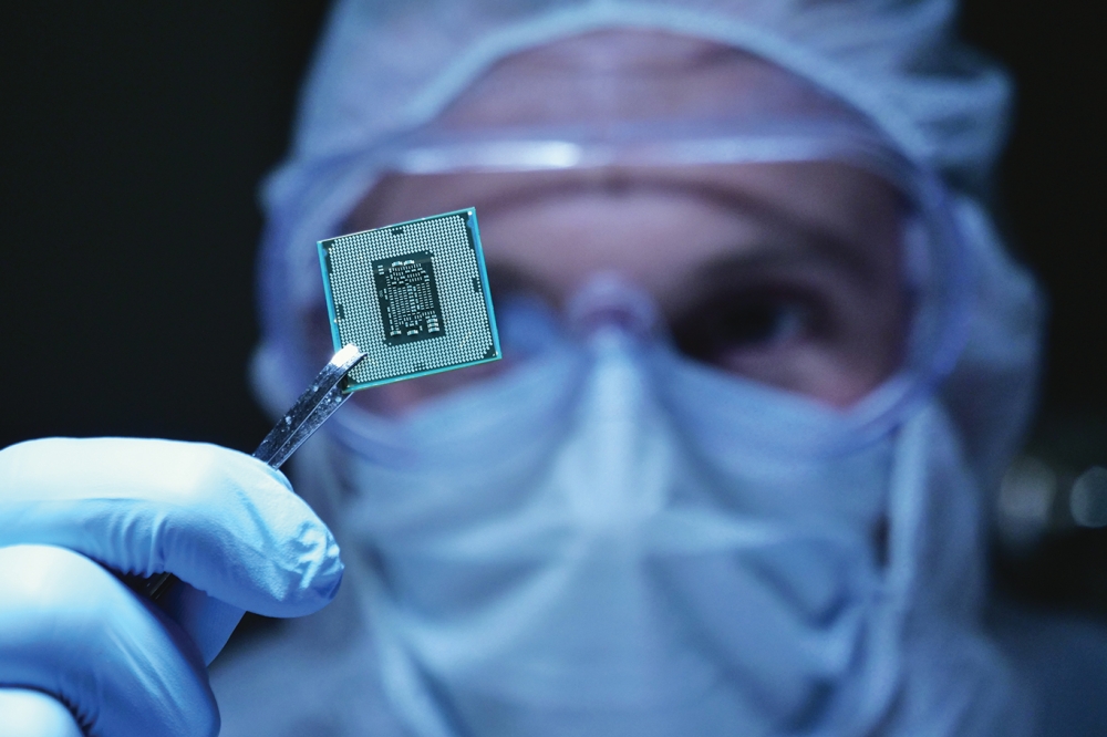
PRINTING CHIPLETS
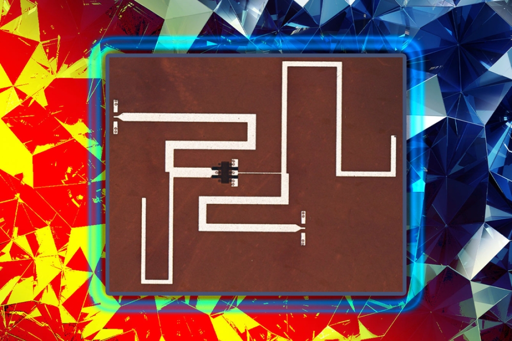
Several situations require moving thousands of chips from their original wafer to another platform. This often takes place when producing displays from red, green and blue microLEDs, and creating concentrating photovoltaic modules equipped with tiny, multi-junction solar cells. Assisting with this task is the inventor of a powerful technique for massive parallel transfer of various devices, John Rogers from the University of Illinois, Urbana-Champaign. He and his co-workers pioneered using rubber stamps to pick up an array of chiplets and deposit them on another substrate. Their first demonstration began by producing single-wall nanotubes, GaN nanobars and silicon wires on separate substrates. Printing these components on a sheet of polyimide created circuits with a bottom layer of GaN HEMTs, followed by single-wall nanotube thin-film transistors and silicon MOSFETs. J. Rogers et al. Science 314 1754 (2006)
GETTING GALLIUM NITRIDE TO THE RED
When LEDs are used to form high-quality white-light sources through colour mixing, or to create the red, green and blue pixels that make up a display, the production process would involves just a single material system. The arsenide family is not an option, because as emission shortens, the bandgap switches from direct to indirect. That makes the only real contender InGaN. While external quantum efficiency in the blue can exceed 80 percent, in the green it is around 50 percent, and for longer wavelengths it is far, far lower. However, there is steady improvement in the orange, yellow and red, with a key milestone reached in 2014, thanks to research at Toshiba. Using an AlGaN interlayer in the active region to reduce the density of energy-sapping defects in the indium-rich quantum wells, this team produced a 629 nm device that broke the 1 mW barrier for a 20 mA drive current. J-I. Hwang et al. Appl. Phys Express 7 0781003 (2014)
WINNING THE GREEN RACE
To participate in the race to make the first green laser, you want access to GaN substrates. That puts those making them at an advantage. Exploiting that to the full came Sumitomo, smashing the record for a long-wavelength nitride laser in the summer of 2009. Until then, teams had built devices on conventional planes or non-polar variants. Sumitomo took a different tack, sporting a semi-polar variant that trims internal electric fields while aiding incorporation of indium in the InGaN quantum wells. First-generation lasers included those producing emission at 531 nm when driven with a 0.5 percent duty cycle. After reporting these results in the August 2009 edition of Applied Physics Express, the team switched from a gain-guided to ridge waveguide design, and a month later reported a 520 nm device with a 2.5 mW continuous-mode output in the same journal. Y. Enya et al. Appl. Phys Express 2 082101 (2009) Y. Yoshizumi et al. Appl. Phys Express 2 092101 (2009)
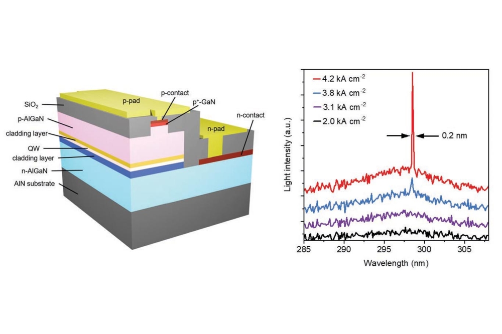
UVC LASER DELIVERS CW EMISSION
Since the fabrication of first GaN laser by Shuji Nakamura in 1995, researchers have devoted much effort to expanding the spectral range of this device. Those striving to reach shorter wavelengths realised a key milestone in 2022, with a team from Asahi Kasei Corporation and Nagoya University producing the first continuous-wave (CW) GaN-based laser emitting in the UVC, which is a spectral range spanning 280 nm to 200 nm. Their 275 nm device, emitting an output power of just over 1 mW, is a promising source for various tasks, including biological and chemical sensing, particle detection, rapid sterilisation, solar-blind communication and materials processing. To produce the first CW UVC laser, the team turned to a novel design that includes polarisation-induced doping, a cladding layer that excels in optical confinement, and a pair of n-type electrodesthat opened the door to lasing. S. Kumar et al. Appl. Phys. Express 15 054001 (2022)
BOOSTING BLOCKING VOLTAGES
When Infineon brought the first SiC Schottky barrier diodes to market in 2001, its pair of offerings could block 300 V and 600 V. The market welcomed these devices, but wanted to see even higher voltages, a feat that could be accomplished given that SiC Schottky barrier diodes had been shown to be capable of blocking 1 kV back in 1994. Those devices, using a palladium metal contact, featured nitrogen-doped, 10 mm-thick layers of 6H-SiC. In the years that followed, 4H-SiC had become available, increasing electron mobility; and researchers had switched to nickel and platinum contacts to realise higher blocking voltages. Drawing on both those advances, in 2003 a partnership between researchers at Rutgers University and United Silicon Carbide broke new ground, fabricating the first SiC junction field-effect transitor that broke the 10 kV barrier. For this class of transitor, their device also broke the record for Baliga’s figure of merit. P. Alexandrov et al. IEE Electronics Lett. 39 1860 (2003)
ERADICATING ELECTRIC FIELDS
Conventional GaN lasers are hampered by the interplay of electrostatic forces and internal stresses that pull electrons in one direction and holes in another, hindering radiative recombination. But this issue can be avoided by turning to new planes for the growth of GaN. Switching to semi-polar planes reduces these fields, and they are eliminated with non-polar planes. Pioneering the later, a team at the University of California, Santa Barbara (USCB), announced the world’s first non-polar GaN laser in a press release on 29 January, 2007. Their bragging rights didn’t last long. Just three days later Rohm revealed that they too had built a non-polar laser – and one with better performance. While the blue-violet laser from UCSB operated in pulsed mode, that from Rohm could produce a continuous output, with a performance comparable or better than conventional GaN diode lasers. K. Okamoto et al. Jpn. J. Appl. Phys. 46 L187 (2007 ) M. C. Schmidt et al. Jpn. J. Appl. Phys. 46 L190 (2007)
BLUE LASER BREAKTHROUGH
Wavelength limits data storage capacity. CDs, read by 780 nm lasers, hold just 780 MB, while DVDs, using shorter-wavelength 650 nm lasers, house up to 4.7 GB. Back in the late 1990s when CD players were in their heyday and DVD players were starting to appear on the high street, every maker of consumer electronics and PCs considered the possibilities of an even shorter wavelength laser chip. And it wouldn’t be long before they could get their hands on such a device, because by then Shuji Nakamura, Nichia’s star, had already laid the groundwork. News of the first GaN laser broke on 12 December, 1995, with details emerging shortly after. Nakamura’s laser emitted at 417 nm, not far from the 405 nm used for Blu-Ray players. His device, providing the shortest emission wavelength for laser diodes made from any material system, started to lase at 1.7 A and produced 215 mW of power at a 2.3 A drive current. S. Nakamura et al. Jpn. J. Appl. Phys. 35 L74 (1996)
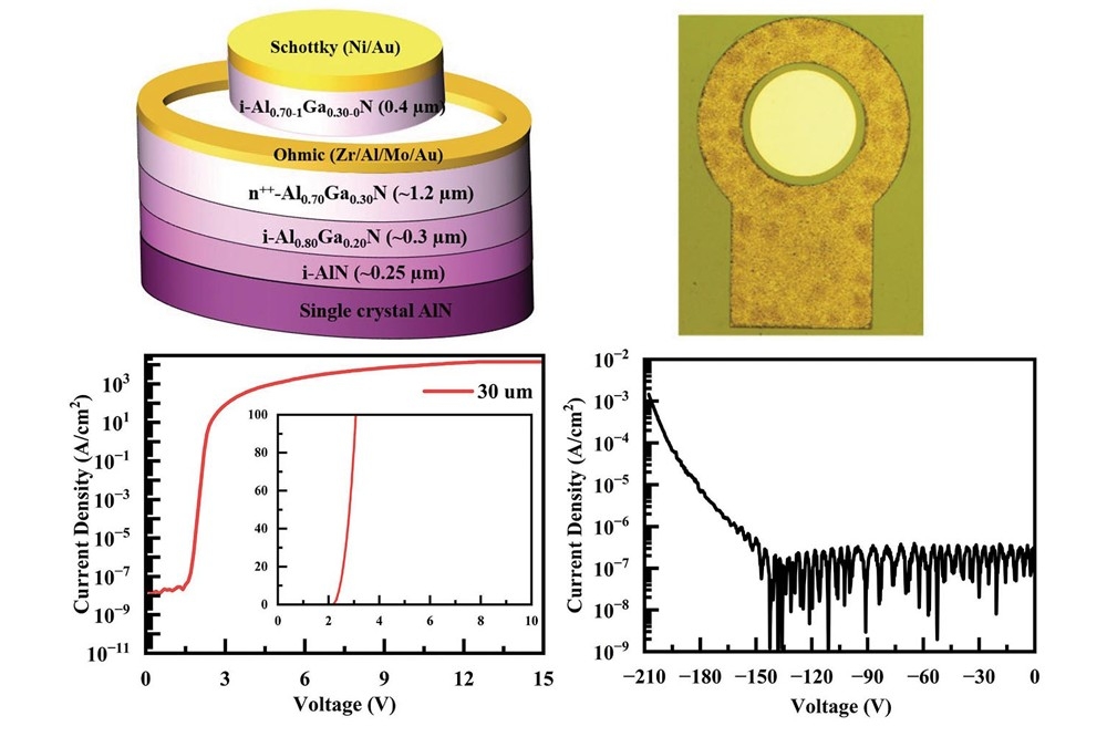
AVALANCHE FOR GAN-ON-SILICON
Devices that offer avalanche capability have much appeal, with benefits that include the provision of a safety margin at the system level, and by operating safely at close to breakdown, an opportunity to use relatively small devices. For GaN HEMTs, a lateral geometry is unable to provide avalanche characteristics, due to a peak electric field in the gate vicinity. This is not an issue with a vertical architecture, with avalanche behaviour initially realised in devices formed on GaN and sapphire substrates. However, native substrates are expensive, and sapphire suffers from a low thermal conductivity. Overcoming these issues, a team from the University of Lille and Siltronic produced GaN-on-silicon devices with avalanche characteristics. To identify this trait, the team plotted the device’s current as a function of reverse bias at different temperatures. These measurements identified the conditions required for impact ionisation, key to avalanche behaviour. Y. Hamdaoui et al. Appl. Phys. Express 17 016503 (2024)