Retrospective - 2015-2025
The last decade will be remembered for a surge in interest in gallium oxide, the creation of the world’s first compound semiconductor cluster, the introduction of the VCSEL into smartphones, and the emergence of the GaN power electronics industry.
Two titans unite
2015. During the last 30 years, the two biggest sectors within our industry, LEDs and GaAs microelectronics, have headed in very different directions. In the LED industry five LED chipmakers rose to the fore in the late 1990s – Nichia, Cree, Lumileds, Toyoda Gosei and Osram – and held on to one of these top spots for many years. Now, though, the LED industry is far more fragmented. In stark contrast, the GaAs microelectronics industry has seen a dramatic contraction in the number of competitors, despite a growth in revenue over the last 30 years from below $0.5 billion to more than ten times this figure.
Big players that have left the GaAs industry include Anadigics, snapped up in 2016 by II-VI (now Coherent), which spent several years converting its RF line to the production of VCSELs. Other leading names have merged.
In 2002, Skyworks formed through the marriage of Alpha Industries and Conexant, and more recently Qorvo emerged from the union of two heavyweights, RFMD and TriQuint. The new entity started trading on 1 January, 2015.
That merger had much going for it. Many viewed the two companies as complementary, with RFMD having greater strength in RF technologies for handsets and TriQuint offering a better portfolio of defence products.
Investors clearly approved of the union, with the share prices of both firms enjoying double-digit jumps on disclosure of the plans. The new entity had the potential to initially net an annual revenue of just over $2 billion; and thanks to synergies providing yearly savings of $150 million, gross and operating margins were tipped to be 45 percent and 25 percent, respectively.
Ten years on, has the merger delivered on all those promises? Well, sales for the four most recent fiscal quarters have amassed $3.24 billion, with a gross margin around the targeted value.
However, the company is currently running at a small loss. This appears to be weighing on the share price, which has fallen from a peak of almost $200 in summer 2021 to around $70, the value of this stock on its first day of trading.
True heavyweight flexes its muscles
2016. If you are a regular reader of his magazine, then by the middle of the last decade you would have been aware of the tremendous promise of gallium oxide. With a whopping bandgap of around 5 eV – the precise value depends on the particular polytype – it has the potential to deliver a knockout blow to those two much-vaunted middleweights, SiC and GaN. Thanks to gallium oxide’s far wider bandgap, it should be able to reign supreme in that most valued of characteristics, the on-resistance as a function of breakdown voltage. But that’s not its only alluring attribute: it offers versatility, because thin films of gallium oxide can be deposited by a variety of techniques, including MBE and MOCVD; and there are several options for the substrate. Devices can be grown on sapphire or gallium oxide, which could tumble in price, because boules of this material can be grown by melt-based techniques.
Gallium oxide’s great promise has made it easy for researchers and developers to attract interest and initial investment. However, like any material, its future hinged on demonstrations of device capability. For gallium oxide, they came thick and fast in 2016.
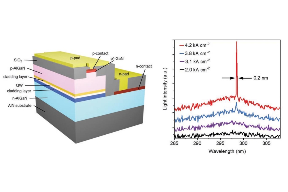
During that year, two key breakthroughs emerged from a team at the Air Force Research Labs (ARFL). Using structures made from the b-polytype and grown on a native substrate, engineers working there grabbed the limelight by producing a MOSFET with a record-breaking critical field strength of 3.8 MV cm-1 – that’s about four times the critical field strength of GaN. And later that year they realised another breakthrough, reporting the first ever enhancement-mode FET with a high-breakdown voltage in the off-state. This second success demonstrated that a lack of p-type carriers in gallium oxide is not a show-stopper to making a normally-off FET. The gallium oxide research programme at ARFL had been inspired by the work at Japan’s National Institute of Information and Communications (NICT). Researchers at NICT, working with domestic partners, had driven much early progress in materials and devices, and gone on to produce the world’s first MESFETs and MOSFETs in 2012.
Japan also provided another milestone in gallium oxide. In 2016, using a novel growth technique known as mist epitaxy, researchers at Flosfia reported β-Ga2O3-on-sapphire Schottky barrier diodes sporting an on-resistance that trumps that of state-of-the-art variants made from SiC. Several years ago, this University of Kyoto spin-off said that it would be commercialising its β-Ga2O3 power devices within a matter of months. The company failed to stick to its schedule, with a market launch postponed by reliability issues. However, it appears that Flosfia is now getting back on track, making progress, having recently announced that it has developed a prototype 600 V, 10 A junction barrier diode that will be sampled to customers this year. This device, with a turn-on of 0.9 V, incorporates p-type (IrGa)2O3. As well as this advance, the company has recently demonstrated the operation of a trench-gate MOSFET and scaled its production processes, establishing β-Ga2O3 growth technology for 4-inch wafers. With plans to also verify 4-inch wafer manufacturing this year, commercial prospects for Ga2O3 are on the up.
Creating the world’s first compound semiconductor cluster
2017. What is the most famous valley in the world? OK, it might not be the first response to trip off your tongue, but a great case can be made for Silicon Valley.
While this region may not have that many fabs today, the engineers that have worked here – many of them, graduates of Stanford University – are to be thanked for not only their advances in technology, but for giving all of us working in the semiconductor industry a higher status in society. Today technology is admired, benefitting many, even if the average man in the street has never heard of holes, bandgaps or lithography.
California is not the only part of the world with a cluster of semiconductor companies. They are also found in Leuven, Belgium; in Dresden, Germany; in Eindhoven, The Netherlands; and in Grenoble, France.
One of the strengths of all these clusters is that by having many companies on each other’s doorstep, often operating at different positions within the supply chain, they are able to support one another while attracting more engineering talent to the region. This helps to boost the kudos of the clusters, bringing in yet more business and innovation, while fostering an entrepreneurial outlook that gives local start-ups the best chance of thriving.
Efforts to create the world’s first compound semiconductor cluster can be traced back to 2011, when IQE’s founder, Drew Nelson, met the economic minister for Wales. Nelson put the case for a far stronger infrastructure within the UK to support the compound semiconductor industry. Back then, IQE had virtually no domestic customers. That’s not to say, however, that IQE was the only company in South Wales working in our industry: this part of the UK was and continues to be home to etching and deposition tool maker SPTS, now part of KLA; and a Microsemi facility with packaging expertise, now known as Microchip Technology Caldicot.
Nelson’s next steps included working within a group set up by the European Commissioner for Technology for the Digital Economy. Involved in a team considering key enabling technologies, he championed the construction of a sovereign capability for compound semiconductors in South Wales, to rebuild the continent’s manufacturing capability for this technology.
Building on these efforts, Nelson lobbied the Welsh Government and Cardiff University to set up an Institute for Compound Semiconductors. He had a vision for a local facility, delivering cutting-edge technology, developed using tools and processes compatible with high-volume manufacturing. In March 2015 the UK Government funded this initiative, and a year on planners gave the go-ahead for the construction of a new building for the Institute for Compound Semiconductors. Forming part of the Innovation Campus, the Institute opened in 2023 after delays partly associated with the pandemic, to play a leading role in the Translational Research Hub.
To help commercialise the technology developed at the Institute for Compound Semiconductors, in 2015 IQE and Cardiff University founded a joint venture: the Compound Semiconductor Centre. Using funding from Cardiff University and some equipment from CSC, it runs collaborative research projects.
In 2016, more links were added to the supply chain. In January, the UK government stumped up £50 million, funding the creation of a Compound Semiconductor Catapult, an open access R&D facility focused on helping UK businesses exploit advances in compound semiconductor technologies. And later that year, the UK’s Engineering and Physical Sciences Research Council poured £10 million into a Manufacturing Hub for Compound Semiconductors, targeting the translation of research into high-volume chip manufacturing.
With many pieces of the jigsaw now in place, in summer 2017 the cluster officially opened for business, taking the name CS Connected and holding events with speakers from all key stakeholders. The cluster also took a huge leap forward, grabbing an opportunity to get its hand on a production line. The 200 mm silicon fab in Newport, South Wales, had come into the hands of Infineon through its acquisition of International Rectifier. After the German powerhouse evaluated its global chip manufacturing capabilities, it viewed the Newport Fab as surplus to requirements. This facility was put up for sale, with Nelson leading a private equity buyout. Emerging from this deal, Newport Wafer Fab had guaranteed orders from Infineon for two years. Further ahead, those in the cluster hoped that the lines would also be used to produce compound semiconductor-on-silicon chips, aided by IQE’s acquisition of Translucent, a developer of rare earth oxides, which can provide a bridge between a silicon wafer and compound semiconductor epilayers.
Further advances within the cluster included the relocation of the CS Catapult to part of a very large building constructed for LG Semicon, with IQE taking the remainder, using it to create an epifoundry that could house up to 100 MOCVD tools. The cluster has also expanded to include Swansea University, which is constructing a Centre for Integrative Semiconductor Materials.
Threatening to derail some of this progress has been the ownership of the Newport facility, which, in 2021, was bought by Nexperia. As Nexperia is a Chinese-owned company, the take-over drew concern from the UK government, which spent many months deliberating over what to do. In November of 2022, the UK government finally came to a decision, ruling that the fab had to be sold. Twelve months on Vishay bought the facility, and late last year announced that it would be investing $51 million in the fab, which will diversify into the production of SiC power devices, and support the growth of the cluster.

Not helped by delays due to Covid, the Institute of Compound Semiconductors, part of the Translational Research Hub, opened in May 2023. Nobel Peace Prize winner and climate scientist Donald Wuebbles presided over the opening.

CSconnected, the world’s first compound semiconductor cluster, opened for business in 2017. By the end of the year this cluster, based in South Wales, had strengthened its capabilities, thanks to the launch of Newport Wafer fab, a facility Infineon deemed surplus to its requirements.
Getting the blues
2018. The VCSEL has a wonderful set of attributes. It is efficient, allowing it to run off a battery; it can be turned on and off at very high speeds, making it a great source for transmitting vast amounts of data; by adjusting the size of the aperture, it can produce single-mode emission with a circular profile, simplifying optics; and it is well-suited to high-volume manufacturing, partly because its design allows on-wafer testing.
However, there is room for improvement. Despites decades of development, the VCSEL spans a far narrower range of wavelengths than edge-emitting lasers and LEDs.
Expansion of the spectral domain has been very slow, given the long history of this device. Its roots go back as far as 1965, when Ivars Melngailis, working in the MIT Lincoln Lab, announced a ‘longitudinal injection laser’ emitting at 5.2 µm, formed from an InSb diode featuring polished top and bottom surfaces to ensure optical feedback. This device, an incredibly impressive feat for its time, is far from practical, with lasing requiring a hefty 20 A drive current and cooling to 10K.
The first real VCSELs came from the labs of Kenicha Iga from Tokyo Institute of Technology. In 1977, Iga proposed a design sharing many of the features of today’s VCSEL, and for the next 11 years he almost singlehandedly pioneered this class of device, before other groups noted his breakthrough and redirected their efforts towards this technology. Success followed, with research in the latter part of the twentieth century initially focusing on the near infrared, before attempts were made to widen the spectral range of the VCSEL in both directions. Initially, breakthroughs with the GaAs-based material system enabled 980 nm and 850 nm VCSELs, before emission stretched to around 650 nm. Wafer-fusion brought yet more success, allowing GaAs-based mirrors to be united with InP-based active regions to realise emission at 1.5 µm.
By the turn of the millennium, researchers started to consider the next goal: expanding emission to the blue and green. Success would open up new markets, allowing devices to be deployed for high-resolution printing, high-density optical data storage, chemical and biological sensing, full-colour displays and lighting.
Producing VCSELs operating in this spectral domain is far from easy. To reach these shorter wavelengths, the GaAs-based material system has to be replaced with one based on GaN and its related alloys. This switch may sound a simple, but it’s anything but.
The biggest issue is producing the mirrors that sit either side of the active region. This is relatively easy in a GaAs-based VCSEL, because this material system is blessed with the pairing of GaAs and AlGaAs. These III-Vs have very similar lattice constants, so strain is not an issue, and there is a significant difference in their refractive index, aiding reflection. When 20 pairs of alternating layers of GaAs and AlGaAs are used to make a mirror, it has a reflectivity of 99 percent, sufficient to make a high-performance VCSEL.
For blue and green VCSELs, to prevent strain from degrading the mirrors, GaN has to be paired with Al0.83In0.17N, a trickier alloy to grow that has a relatively low refractive index contrast. Growing two sets of GaN-based mirrors would take too long, so it is better to combine a nitride-based bottom mirror with a top one based on dielectrics, an approach pioneered by Nicholas Grandjean’s team at EPFL. Their high-point came in 2007, when they reported the first optically pumped GaN VCSEL.
Frustratingly, funding dried up for Grandjean, with those holding the purse strings arguing that the first electrical VCSEL would come from Japan. They were more or less right, and now we will never know if Europe could have been the trailblazer of this device.
The first electrically pumped GaN VCSEL actually came from National Chaio Tung University, Taiwan, announced in April 2008. This required cryogenic cooling, a restraint overcome later that year by Nichia, using a pair of dielectric mirrors. Nichia persisted with this design, increasing the output power to 0.62 mW in 2009. Over the next few years it continued to develop this device, but only realised minor additional gains.
Substantial progress came in 2018, when two Japanese companies, working independently, broke the 10 mW barrier – this is roughly the power required for augmented-reality devices, projection systems and displays. Stanley Electric, partnering with Tetsuya Takeuchi and his team from Meijo University, built on the work at EPFL, improving the growth conditions. In the autumn of that year, they reported a blue VCSEL with an output in excess of 15 mW. And in November 2018, Sony unveiled a 12 mW VCSEL with a novel design, featuring a far larger cavity that incorporates a thinned GaN substrate, and a curved mirror grown on the backside of the wafer.
Since then, gains have been modest, with the most powerful GaN VCSELs now emitting just over 20 mW.
Alongside the breakthroughs in blue VCSEL performance, 2018 will be remembered for the market success of infrared cousins. Up until then, datacoms provided by the primary revenue stream for this device. However, in 2018 the market for handsets caught up, thanks to Apple’s launch of the iPhone X. This smartphone featured two VCSELs: one for the dot projector, and another for the flood illuminator.
Many rivals in the smartphone sector also launched new models that incorporated VCSELs, used as the light source for time-of-flight technologies to avoid any potential IP issues. These sales have dwindled over the last few years, as makers of Android-based smartphones have tended to ditch the VCSEL in their latest models to free up space for the introduction of components for 5G networks. However, despite this loss of business, VCSEL revenue for the consumer electronic market is still increasing.
When Apple started to deploy VCSELs in its smartphones, Lumentum provided this device. But to reduce supply chain risk by adding a second source, in late 2017 Apple encouraged Finisar to become a VCSEL supplier, promising orders totalling $390 million, with the US manufacturer grabbing this opportunity. Over the intervening years Finisar’s VCSEL production business has been acquired by II-VI and subsequently incorporated into Coherent, which now has a significant share of the market.
For the last few years, Coherent and Lumentum have been competing for Apple’s business with Trumpf Photonic Components. Recently this chipmaker, which has shipped over 1 billion VCSELs to Apple, has been expandeing its manufacturing facilities for this device at its site in Ulm, Germany, which it bought from Philips Photonics in 2019.
Sales of VCSELs to the datacom market are now outpacing those for consumer electronics. Due to this, in 2022 Yole forecast that the datacom market would be overtaking that for consumer electronics. But more recent trends suggest that consumer electronics will remain the biggest market by far, accounting for $974 million in 2028, compared with $232 million for the telecom and infrastructure sector.
Several years ago, it looked like lidar for autonomous vehicles would be the next killer application for the VCSEL. However, the introduction of self-driving cars has been hampered by safety concerns, and here the VCSEL has come up against strong competition from fibre lasers and edge-emitting lasers, with the latter having the lion’s share of this market. This led Yole to predict that by 2028 VCSEL sales to the automotive and mobility market will net just $108 million, a relatively small slice of the $1.4 billion expected that year.

To secure a second source for VCSELs, Apple agreed to purchase $390 million of these devices from Finisar.

Facial recognition offers a lucrative market for the infrared VCSEL.
A phenomenal cash injection for silicon carbide
2019. In spring 2019, Cree, now Wolfspeed, re-aligned its business in emphatic fashion. It’s relatively new CEO Greg Lowe had no qualms in carving of the company’s Lighting Products division to Ideal Industries; giving the LED business that brought so many years of success a back seat; and focusing on wide bandgap materials, and RF and power devices. Helping to have made this monumental decision would have been a number of lucrative SiC wafer supply deals: contracts with Infineon, ST Microlectronics and other companies totalled $500 million.
By summer 2019 the company’s LED business had softened and it had netted the lion’s share of its $310 million sale to Ideal. These circumstances would have helped Lowe to move forward with his vision, investing $1 billion in massive expansion of SiC capacity. A state-of-the-art, 200 mm facility would be built by 2024, delivering a 30-fold expansion in capacity compared with the first fiscal quarter 2017.
Later that year the company had an offer it could not turn down – a $500 million grant from the state of New York. Instead of having to spend $450 million retrofitting existing infrastructure at its headquarters in Durham, NC, it could now invest $170 million in building a new, automotive-qualified 200 mm power and RF wafer fabrication plant in Marcy, New York. And instead of ramping up capacity by a factor of 30, it would go up 40 times.
Opened in April 2022 to much fanfare, Wolfspeed described this facility during its christening as ‘the first, largest and only 200 mm SiC fab in the world’. Back then, the company rode the crest of a wave, with many bold plans, plenty of backers, and a share price of over $100. But since then, the share price has tumbled, now trading well below $10, as the company has struggled from sluggish growth in the electric vehicle market, while facing increased competition from rival producers of SiC substrates, particularly from China. Last October Wolfspeed shelved plans to build the world’s most advanced SiC manufacturing facility in Saarland, Germany, and now it’s trimming its workforce by a fifth in a bid to cut costs. Amongst those redundancies is Greg Lowe, axed in November. The company is now seeking a new leader to transform its fortunes.

On 25 April, 2022, the day that Wolfspeed opened its 200 mm automotive-qualified SiC fab in Mohawk Valley, Upstate New York, the SiC tech supplier also announced a multi-year agreement with Lucid Motors, to supply SiC power semiconductors. These devices have been deployed in the luxury, all-electric Lucid Air.
Covid’s silver lining
2020. Who will forget 2020, a year that will go down in history as one when a pandemic rocked the world, with the rapid spread of Covid-19 having devasting consequences. As well as a high death toll – according the World Health Organisation, fatalities totalled more than 3 million – economies everywhere faced immense strain as the citizens of many nations were forced to isolate, sparking mental health issues with consequences lingering to this day.
While government rulings led many to work from home, those playing a hands-on role in semiconductor industries were seen in a different light. Compound semiconductor facilities continued to churn out chips around the clock, and even benefitted from opportunities associated within this global crisis.
To minimise loss of life, scientists devoted a great deal of effort to the speedy development and roll-out of a vaccine. And in addition to pursuing this game-changer, solutions were sought to kill this virus.
An attractive approach to dis-arming the virus is to subject it to emission from a deep-UV light source. The incumbent option, the mercury lamp, is bulky, fragile, requires a high operating voltage, and is plagued by environmental concerns. One way to address all these weaknesses is to switch to a battalion of deep-UV LEDs. Although they lag the performance of their blue-emitting cousins, they promise to come on in leaps and bounds through greater investment, spurred on by lucrative applications.
During the pandemic, interest in deep-UV LEDs skyrocketed, with firms launching new devices, alongside specialist growth tools and various disinfection systems.
Powerful deep-UV LEDs are far harder to produce than those emitting in the visible, due to a variety of issues, including realising sufficient light extraction and high enough levels of doping. Due to these and other challenges, the established makers of these devices were best-placed to ramp volumes, such as the partnership between Sensor Electronic Technology and Seoul Viosys, a subsidiary of Seoul Semiconductor. During the height of the pandemic, this collaboration started mass-producing UV LED modules that could sterilise 99.9 percent of the coronavirus within 3 seconds. In addition, they began developing a Photon Shower, described as a whole-body sterilisation solution that could sterilise germs on people’s clothing in a matter of seconds.
To support companies trying to manufacture the deep-UV LED, the Chinese equipment manufacturer AMEC launched a new MOCVD tool, the Prismo HiT3, said to be ideal for producing high-quality layers of AlN, a key material for this short-wavelength source.
During the height of lockdown, new disinfection systems employing deep-UV LEDs were also launched to market. Over the summer of 2020, water-treatment specialist AquiSense launched a surface disinfection system, and Singapore-based robotics manufacturer, Ostaw Digital, unveiled what was claimed to be the world’s first disinfection robot using LEDs emitting at appropriate wavelengths. When fully charged, this autonomous robot could be deployed for 5 hours, delivering a disinfection rate of 99.999 percent at a range of 2.5 m.
Sales of deep-UV LEDs emitting at wavelengths suitable for sterilising Covid-19 shot up during 2020, according to market analyst Yole, with revenue almost doubling year-over-year to $308 million. But that’s still well short of the value of the visible LED market, and even if the pandemic has provided a catalyst for healthy long-term growth of this source of deep-UV emission, this device is going to be valued more for its importance than its sales.

In summer 2020, at the height of the Covid-19 pandemic, Ostaw Digital claimed that it had introduced the world’s first disinfection robot using deep-UV LEDs.
Valuing vertical integration
2021. When do you think our industry began to manufacture devices in high volumes? While it’s a question without a definitive answer, a strong case can be made for the late 1990s, a time when fabs started to crank up production of GaAs transistors and GaN LEDs, two key devices for the growing handset market.
To produce LEDs, fabs tended to buy sapphire substrates, carry out epitaxial growth and processing in-house, and send the die to a packaging partner. While with the GaAs HBT, two routes were common, with epitaxial growth either outsourced or undertaken by the chipmaker.
For manufacturers of both LEDs and GaAs HBTs, what was beyond question was the production of the substrate. This task would be undertaken by a company dedicated to growing crystals, slicing them, and polishing the resulting substrates, so that they provided a high-quality foundation for epi-growth.
With SiC, supply chains are far more varied. As SiC cannot be grown from the melt, producing high-quality substrates is far from easy, accounting for the relatively slow progress of devices from the lab to the fab. For chipmakers, getting their hands on a sufficient supply of high-quality substrates has been crucial to making high-performance devices, so when many have wanted to ramp production over the last few years, they have had to negotiate wafer supply agreements.
SiC device pioneer Cree, now Wolfspeed, has met some of this demand. This company has benefitted from using SiC substrates as the foundation for its LED production, a modus operandi that has led to a wealth of SiC substrate expertise, derived from producing a product in volume. Higher-quality SiC substrates have resulted, providing a great platform for internal development and commercialisation of SiC power devices.
After looking on in envy at Wolfspeed, many of the other leading makers of SiC diodes and MOSFETs are now bringing matters into their own hands by developing vertically integrated production capabilities that begin with the production of SiC substrates, or even the refining of powders used in their production.
Significant strides in pivoting to extensive vertical integration were taken by many of the big players in SiC power electronics in 2021. They included one of Wolfspeed’s long-term rivals, Rohm, which completed its construction of a $190 million SiC wafer and device production plant in Chikugo, Japan, that promised to lead to a five-fold hike in chip production. Prior to this, Rohm acquired the German SiC wafer manufacturer, SiCrystal, in 2019.
Another noteworthy move came from China, with the opening of Sanan IC’s manufacturing fab, a $2.3 billion facility that combines crystal growth with the production of power devices and their packaging and testing. Constructed in phases, chip production began with 15,000 6-inch wafers per month, and there are long-term plans to move to 40,000 8-inch wafers.
Onsemi also grabbed the headlines in 2021 with the $415 million acquisition of the US producer of 6-inch and 8-inch SiC material GT Advanced Technologies. Motivations behind this move were to secure and grow Onsemi’s supply of SiC, and to meet a growing demand for SiC power electronic devices for electric vehicles and energy infrastructure.
The trend for extensive vertical integration by the biggest players in SiC power devices continues to this day. In late 2022 STMicroelectronics announced that it would be making SiC substrates at its site in Catania, Sicily. The company planned to make a €730 million investment over 5 years, with SiC substrate production expected to begin in 2023. To much fanfare, STMicroelectronics announced further investment of €5 billion in this site last year. In May 2024, supported by €2 billion from the State of Italy in the framework of the EU Chips Act, funding is now enabling the construction of a vertically integrated 200 mm SiC campus, which includes SiC substrate development, epitaxial growth processes, front-end wafer fabrication, module back-end assembly, and a number of R&D initiatives. Production of SiC products at this campus is set to start in 2026, and ramp to full-capacity by 2033, enabling the processing of 15,000 wafers per week.

Sanan IC’s manufacturing fab, located at the Changsha high-tech industrial plant, is China’s first vertically integrated SiC line.
Power GaN’s inflection point?
2022. For many emerging devices, commercial success is anything but linear. Initial breakthroughs are far from easy, with much effort having to be devoted to convincing potential customers that there is much to gain by adopting a new chip. But if this leads to success, other firms will follow, swelling the sales of this device and demonstrating its prowess. This platform can then provide a foundation for further success, as device deployment branches out into a number of new applications.
For the GaN power device, that inflection point came around 2022, with many of its producers targeting new markets by expanding their portfolio or ramping production. An uptake of GaN HEMTs in mobile chargers, where they enabled far shorter charging times, provided the bedrock for the expansion of this device into new markets. During the summer of 2022, Yole forecast that the consumer power market would expand at a compound annual growth rate of 52 percent between 2021 and 2027 to hit $915 million, and by the end of that timeframe global GaN revenue would total $2 billion. According to the French analyst, power supplies for telecom and datacom would provide substantial, fast-growing sales, with revenue tipped to climb to $620 million by 2027. Helping to secure revenue from this sector were design wins for Transphorm, EPC, Texas Instruments, Infineon and GaN Systems.
By 2022, GaN Systems, now part of Infineon, had also made significant progress in the automotive market, amassing contracts from BMW and Toyota, Canadian GaN powertrain developer FTEX, and EV powertrain system supplier Vitesco Technologies. In addition, GaN Systems had just secured $150 million of investment from BMW i Ventures, Vitesco and other players.
Speaking to Compound Semiconductor in early 2022, Jim Witham, then CEO at GaN Systems – and now Senior Vice President at Infineon Technologies – argued that the tremendous high-frequency capabilities of GaN power devices could spur success in on-board chargers and DC-to-DC converters in electric vehicles. He also claimed that GaN could compete with SiC for success in the traction inverter.
The Chinese GaN chipmaker Innoscience also eyed new opportunities in 2022, the year it opened sales offices in the US and Europe and planned to ramp production capacity from its 8-inch fabs in Zhuhai and Suzhou from 10,000 to 14,000 wafers per month. Dominated by sales to makers of fast chargers, this company targeted revenue from DC-to-DC converters in data centres, LED drivers, lidar laser drivers and DC-to-DC conversion in electric vehicles. Looking further ahead, 650 V on-board chargers were viewed as another opportunity.
Other producers of GaN HEMTs pursuing new markets in 2022 included: Rohm, releasing a 150 V HEMT for power supplies in base stations and data centres; EPC, introducing demonstration boards for radiation-hard GaN power devices that could be deployed in space applications; and Navitas, launching GaNSense, a GaN half-bridge power IC. The latter product, claimed to break new ground through the monolithic integration of a gate driver, a power device and sensing and protection functionality, promised to maintain Navitas’ position as the leading supplier of GaN power devices. Back then, Navitas’ devices were in more than 150 different charging products from different companies, and opportunities had been identified in the solar, data centre and electric vehicle sectors.
2022 also witnessed the start of the transformation of a European silicon fab into one for producing GaN devices. In February of that year, the BelGaN Group bought the fab in Oudenaarde, Belgium, from Onsemi, with the aim of becoming a leading 6-inch and 8-inch GaN automotive foundry in Europe. However, it’s not been a story of success for this venture, with BelGaN filing for bankruptcy last summer, putting 440 jobs at risk.

Bought from Onsemi, BelGaN had big ambitions for the Oudenaarde fab, planned to be converted to the production of GaN power devices for the automotive industry. But these dreams have not been fulfilled, with BelGaN filing for bankruptcy in July 2024.
A new GaN patents war
2023. When it comes to GaN, it seems that the HEMT is following a similar trajectory to that of the LED. In the early days of the high-brightness, GaN-based LED, many companies focused on expanding their portfolio to win lucrative contracts. But once sales had climbed, these chipmakers started to look beyond building better devices, and began waging war with one another, claiming infringement of key patents. Come 2023, history started to repeat itself, triggered by surging sales of GaN power devices.
The first significant shots in the GaN HEMT patent war were fired in May 2023, when the Californian fabless firm EPC issued a press release stating that it had sued Chinese chipmaker Innoscience for infringing four of its US patents. EPC claimed that Innoscience drew on this IP for the production of its 100 V and 650 V products. As well as filing complaints in the federal court and with the US International Trade Commission (ITC), EPC publicly accused Innoscience of poaching two employees that went on to be that chipmaker’s CTO and Head of Sales and Marketing – hires said to be behind the launch of very similar products. Innoscience fired back just two days later with a press release claiming innocence, following an internal investigating involving a thorough analysis and finding no infringement.
However, what matters in this war is not the scoring of points in press releases, but producing winning arguments in court, based on the fine print within the patents.
The battle between EPC and Innoscience concerns a particular form of HEMT produced by both parties, a normally off (E-mode) variant featuring a p-doped layer of (Al)GaN under the gate of the device.
Initially, EPC’s action against Innoscience involved four patents – two from 2013, and another two from 2017. However, EPC dropped the latter two patents in its ITC case.
One of the two contested patents, US 8,350,294, concerns the design and fabrication of a compensated gate MISFET. Here a key issue is whether the phrase ‘compensated GaN layer’ describes the gate layer in Innoscience’s devices, presumably formed by doping GaN with magnesium. Realising effective p-type doping is far from trivial, having been a key milestone in the development of the LED.
EPC’s other patent taken to court, US 8,404,508, is associated with a self-aligned gate E-mode HEMT. That patent describes a multi-step process involving the use of three different photoresist patterns to produce a self-aligned gate.
Initial rulings in the summer of 2024 by the administrative law judge (ALJ) in the ITC case found that both of EPC’s patents are not invalid, and significantly, that the ‘294 patent is infringed. Another blow to Innoscience came from rulings that counterpart Chinese EPC patents were not invalid.
Last November, the ITC affirmed its initial determination that Innoscience infringed the ‘294 patent, a decision leading to a ban on Innoscience from importing GaN-related products into the US without a license from EPC. A 60-day Presidential review period followed, completed this January, leading to a final determination by the ITC that Innoscience cannot import and sell its products in the US without a license from EPC.
Additional action against Innoscience has been taken by Infineon, which began by bringing a suit in San Francisco in March 2024 for a patent associated with high-voltage packages featuring so-called ‘source sensing’. Innoscience responded by filing a petition in June with the US Patent Office, arguing for invalidation of every single claim. Stepping up its attacks over the summer, Infineon filed several cases in Germany, obtaining a preliminary injunction that prevented a small fraction of Innoscience’s high-voltage GaN transistors from being promoted at PCIM. The German powerhouse also added three more patents to the San Francisco case, and filed its own complaint with the ITC.
One of these three additional patents is concerned with the thickness of a titanium nitride capping layer in an electrode stack, and the other two are related to so-called ‘merged cascode transistors’.
Patents battles are sure to be in the news this year. This January Innoscience filed a lawsuit against Infineon related to a GaN power device and its manufacturing method, and in the autumn the AJC will make an initial ruling on Infineon’s accusations against Infineon. It would be surprising if these actions were to be the last between makers of GaN power devices, given that revenue is rising fast, and more players are entering the field. The history of the LED suggests that the patent war will rage on, and it’s hard to foresee a different outcome.
Catching up with silicon
2024. Within the semiconductor industry, a well-trodden path to realising economies of scale is to increase the size of the wafers. Silicon has led the way, migrating from 1-inch to 6-inch wafers from the 1960s to the 1990s, shifting to 200 mm by the start of the millennium, and 300 mm becoming increasingly common from the 2010s. But there it has stayed.
Our industry, often in the shadow of silicon, is now catching up. Leading the way is our power electronics sector, which made great strides in 2024. During the latter part of that year, Infineon claimed development of the first 300 mm power GaN technology, and Chinese provider of SiC substrates, SICC, demonstrated what appeared to be the first 300 mm SiC substrate.
As the production of today’s GaN-on-silicon HEMTs uses substrates with a diameter of 200 mm or less, Infineon’s breakthrough opens the door to more than doubling the number of devices per wafer. But that’s not the only gain that will trim the cost of production, with migration to larger wafers providing improvements to the manufacturing process, such as a higher yield and access to superior metrology. Engineers at Infineon enjoyed these benefits when progressing from 150 mm to 200 mm wafers, and they are seeing them again in the move to the 300 mm platform.
Requiring 18 months of development, Infineon’s 300 mm process, built on its 200 mm GaN-on-silicon technology, is claimed to offers the tantalising prospect of reaching cost parity with silicon equivalents. Helping to reach this goal will be: economies-of-scale; improvements in the technology itself, particularly the epitaxial stack; and the lower on-resistance of GaN, enabling smaller die to deliver the same performance as comparable products made from silicon.
The growth of 300 mm epiwafers is challenging, with differences in lattice constant and thermal mismatch threatening to lead to bowing and even cracking. These issues are exacerbated for thicker layers of GaN, required for higher blocking voltages. While a path to progressing from 100 V to 650 V has been identified by Infineon, going beyond that will be more challenging, with a switch to thicker substrates a possible solution.
At the Electonica show, held in Munch in mid-November, Infineon released its next-generation G5 HV technology. The German powerhouse is planning to take this process and apply it to 300 mm wafers, with engineering samples reaching customers by the end of this year, and production ramping in 2026.
SICC, the world’s second biggest producer of SiC, also selected Electronica to showcase its triumph – the world’s first 300 mm SiC substrate, cut from a 20 mm-thick boule n-type formed using the same axial growth rate employed for manufacturing 200 mm material.
Historically, SiC substrates have been plagued with a variety of imperfections that degrade and even kill devices. However, these issues have now been addressed by many companies, and as the process that SICC employed to fabricate its 300 mm substrate is the same as that used to produce smaller wafers, there is no major barrier to realising state-of-the-art quality with the larger format.
Characterisation of SICC’s ground-breaking 300 mm substrate has revealed that micropipes, a critical defect, are not a significant issue, and surface roughness is comparable to that for the company’s 200 mm wafers. Of more concern are basal plane dislocations, which need to be reduced.
However, the company is confident it can replicate the density found on its 200 mm n-type substrates.
The timing of SICC’s commercialisation of its 300 mm n-type SiC substrates will be governed by the rate of technical progress of this new format and the level of demand. The expectation is for small production volumes to begin in 2027.

In the autumn of 2024 Infineon claimed to have developed the first 300 mm power GaN technology, which promises to enable cost-parity with silicon devices.
Is now the moment for the microLED?
2025. In the depths of winter, it’s far from easy to determine what will be the most significant milestone for the compound semiconductor industry this year. But based on some of the headlines from the recent Consumer Electronics Show (CES), maybe, just maybe, this will year that the microLED starts to fulfil its commercial potential and generate significant sales.
This tiny emitter has certainly had its setbacks over the last few years. As well as falling short of some of the more optimistic forecasts from market analysts, it has faced what might have been a devasting blow last February, when Apple decided to terminate its supply deal with ams Osram.
Apple’s move, a decision that drove the European chipmaker to consider selling its second fab in Malaysia, has had widespread implications, because Apple played a major role within this space for many years. Arguably, this tech giant created the microLED industry through the acquisition of start-up Luxvue in 2014. This move provided the catalyst for investing in the technology by dozens of startups, as well as most OEMs and display makers.
Although Apple’s decision sent shock waves through the microLED industry, those carefully following developments could have anticipated this outcome. There have been multiple slips in Osram’s microLED fab ramp-up timeline, indicating that Apple and its other partners were encountering problems and delays downstream, especially with the mass transfer and assembly of the microLED on the backplane, as well as overall process integration. What’s more, yields remained low, hampering efforts to reach cost targets.
In the aftermath of Apple’s exit from the microLED industry, its epicentre has shifted to Taiwan, which has a strong domestic ecosystem, thanks to AUO and PlayNitride.
Recent highlights for those two companies include AOU’s demonstration of a 17.3-inch foldable display last May at Display Week 2024, and its construction of a new production line for producing automotive displays, which are expected to launch by 2026 or 2027. PlayNitride’s progress is seen in its qualification of a Veeco Lumina MOCVD system for the production of microLEDs, and orders for two of these tools, to be delivered this year.
At CES, attendees were reminded that while Taiwan may be the leader in commercialising microLEDs, it is a global industry. At that show French microLED maker Aledia announced that it has used its nanowire technology to develop a microLED microdisplay with monolithic red, green and blue microLEDs produced on the same substrate that deliver ground-breaking efficiencies. And Canadian firm VueReal used CES to promote its microLED design reference kits, claimed to accelerate the adoption of microLED technology.
Also making headlines this January has been UK-based microLED maker Plessey, which is working with meta. Plessey has just claimed to have produced the brightest red microLED display suitable for AR glasses, a triumph that’s claimed to pave the way to the next computing platform.
While all these breakthroughs are encouraging for the future of the microLED, I cannot argue that they will guarantee success. As the incumbent OLED technology is improving all the time, 2025 may well be a year of now or never for the microLED, determining the future for this miniature marvel.

This January, UK-based microLED maker Plessey, which is working with meta, claimed to have produced the brightest red microLED display that’s suitable for AR glasses.