
GaN-based lasers for quantum applications
Blue lasers with surface gratings are delivering quantum precision from millimetre footprints.
BY RYAN ANDERSON FROM BLUGLASS
The visible spectrum is an exciting frontier for laser diode technology. Here emerging applications exist, demanding sources with a small size, low power consumption and high-fidelity.
Addressing this need are narrow-linewidth lasers. Capable of single-frequency emission, these emitters enable breakthroughs in quantum computing, quantum sensing, and secure communications.
For those in search of a narrow-linewidth laser, an attractive candidate is the GaN-based distributed feedback (DFB) laser, a device we have developed at BluGlass. We view this source as a significant step in the progress of narrow-linewidth lasers, because our device combines a compact form with a relatively straightforward manufacturing process and a level of performance that promises to drive innovation in visible photonics.

A bar with 12 high power GaN laser chips on a USB stick for size
comparison. The optical microscope image is a higher magnification of a
single chip.
Precision emission
For every laser, its spectral linewidth has a profound impact on how it interacts with its environment. When the linewidth is narrow, nearly all emitted energy is concentrated into a useful optical frequency. That’s a massive asset when serving in an atomic system, as this exactness makes the difference between realising the resonance for laser cooling or missing the absorption line entirely.
Quantum technologies, which depend on a high degree of accuracy and precision, rely on the excitation of sensitive atomic transitions by lasers emitting at specific wavelengths. Within this sector, Rydberg sensors are emerging as power detectors for electric fields. These sensors, requiring visible light with linewidths of hundreds of kilohertz, can target many applications, ranging from high-resolution RF imaging and communication and surveillance to quantum computing and networks for defence and aerospace.
In addition to quantum applications, lasers emitting in the blue and green are compelling candidates for underwater communications and lidar, thanks to operation in the spectral sweet spot for water penetration. Similarly, these wavelengths can provide the optical source for remote detection of aerosols, gases, and clear-air turbulence, helping scientists understand weather patterns and pilots avoid dangerous flightpaths in otherwise impossible-to-detect conditions.
In all these applications, one theme is clear: there’s a need for compact, stable, scalable narrow-linewidth sources in the visible regime.

The difference between a single-frequency laser and typical Fabry-Pérot
laser diode are starkly evident when comparing the spectral
characteristics measured in an optical spectrum analyser. The width of
the DFB laser is less than 3 picometers and limited by the resolution of
the measurement system, while the Fabry-Perot laser is approximately
0.5 nm.
Comparing options
The narrow-linewidth laser can take various forms, all involving significant trade-offs between performance, complexity and practicality.
In general, external cavity diode lasers are a well-established source with an excellent linewidth. Incorporating tuneable optical cavities outside the laser medium, this class of laser requires quite sophisticated precision optics. This often results in bulky but delicate benchtop systems, needing alignment, isolation, and complex packaging.
Another promising approach for compact visible lasers are photonic integrated circuits (PICs) featuring GaN emitters. In this configuration, a laser gain section is fabricated on a chip that couples the optical output into waveguides, with external resonators or filters controlling the emission frequency. GaN-based lasers featuring a ring resonator as a PIC have produced impressively narrow linewidths, but at the expense of complex wafer bonding and multi-step processing. Each additional layer of integration may double or triple fabrication complexity.
We are trailblazing a third route: the GaN distributed feedback (DFB) laser. This design, already well-established in lasers made from traditional III-Vs, uses a precisely defined grating that’s built into the optical cavity to select and stabilise a single-emission wavelength. While DFBs are yet match the sub-100 kHz linewidths of the most advanced PIC-based systems, they offer a balance of performance, size, and manufacturability practical for large-scale deployment.
In our view, all three classes of narrow-linewidth laser have a role to play in the application landscape. Here, the GaN DFBs occupy the critical middle ground, as they are simpler than external-cavity diode lasers and cheaper than heterogeneous PICs, while still delivering narrow linewidths and a stability sufficient for most quantum and sensing applications.

Light output for a master-oscillator and power amplifier configured
laser diode. The inset exhibits the narrow linewidth spectral peak and
the associated far-field mode profile at 400 mW of output power. The
test is performed under quasi-continuous wave electrical injection.
GaN DFB challenges
Replicating the processes employed for making III-V DFB lasers with a GaN-based material systems is far from trivial. The primary challenge stems from difficult epitaxial layer growth in the III-nitride hexagonal material system. With conventional III-V DFB lasers, fabrication involves overgrowth of patterned semiconductor layers, a step that’s typically straightforward in a cubic material system. In stark contrast, regrowing GaN over etched gratings tends to introduce defects or roughness, compromising optical and electrical performance.
To address this concern, some groups turn to porous GaN layers or laterally etched gratings. However, impressive results are realised with methods that add complexity or introduce new limitations.
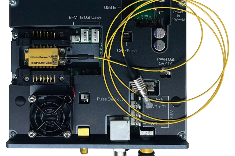
We have developed a different approach that avoids deep etching and regrowth entirely. Instead, we form embedded surface gratings in the transparent, conductive material indium tin oxide (ITO).
With our approach, after epitaxial growth of our GaN laser structure, we deposit ITO as a transparent p-contact. We then define nanoscale gratings in this oxide by electron-beam lithography. After writing them, they are directly embedded under another thin ITO layer to preserve a smooth, conductive surface for current spreading.
This design, originally developed at the University of California, Santa Barbara (UCSB), and refined through our ongoing collaboration, avoids the most challenging aspects of GaN fabrication. It minimises damage to the p-GaN layer, maintains optical quality, and integrates the feedback mechanism directly within the device’s current-spreading layer.

Chip types manufactured by BluGlass from left to right including basic Fabry-Pérot lasers, DFBs, semi-conductor optical amplifiers, single spatial mode MOPAs, and high-power single-frequency lasers
Record-breaking linewidths
Over the last few years our team has made significant strides in optimising the epitaxial structure and the embedded grating design. By refining the optical mode overlap and the coupling strength, we’ve realised side-mode suppression ratios (SMSRs) exceeding 40 dB, a clear indication of single-mode operation.
An even more impressive result is a linewidth of just 680 kHz, recorded when UCSB researchers measured the fundamental linewidth of our embedded-grating GaN DFB laser using a correlated self-heterodyne setup. To our knowledge, this is the narrowest fundamental linewidth reported for a nitride-based DFB laser.
Thanks to this result, we know that our GaN DFBs are within the performance range for laser cooling, atomic sensing and visible lidar applications – and they are within striking distance of 100 kHz, which could open the door to even more demanding quantum technologies.
Wavelength tuning
Linewidth is not the only critical characteristic for a single-frequency laser. It’s also essential that accuracy and precision hit a bullseye regarding the target wavelength of a particular application; and the laser runs at a stable wavelength under a wide range of operating conditions.
To consider these criteria, we’ve compared our DFBs against Fabry-Pérot lasers from the same wafer, operating under varying temperatures and currents. Under those conditions, our lasers maintain single-mode operation and shift by only 17 picometers per degree Celsius. This is a remarkably low sensitivity to temperature compared with traditional III-V lasers. Our DFBs also exhibit a very low wavelength drift during current sweep.
This robustness makes our sources ideal for portable applications, where environmental control isn’t perfect.
For some applications it’s essential to provide a modest tunability, on the order of a few nanometres – this feature enables locking to atomic transitions. It is challenging to meet this need with GaN, due to a relatively stable refractive index with temperature; and it’s also not easy to take the well-trodden path of adding regrown passive phase sections, to create a device that’s similar to an external cavity.
As a first step towards coarse tunability, we have explored prototypes with two cavities resembling distributed Bragg reflector lasers. While these devices undergo mode hops during current adjustment, we are optimistic that clever design will enable pathways for realising controlled tuning in multi-section lasers. Through ongoing work, we are aiming to refine these structures and explore three-section architectures that combine stability with electronic control.

The relative peaks and magnitudes of various devices manufactured by BluGlass under current in the violet wavelength regime.
Scaling-up power
Many applications require not just stable light, but a lot of it. We have already demonstrated DFBs with up to 100 mW of single-frequency emission, and we are pushing toward hundreds of milliwatts and beyond, via the introduction of semiconductor optical amplifiers and configurations that include master oscillator power amplifiers.
To create efficient amplifiers, we’ve developed anti-reflective coatings that have a reflectivity of less than 0.1 percent at 450 nm. According to initial tests, amplifiers with these coatings, which prevent unwanted feedback and lasing modes in the external cavity, provide up to 15 dB of optical gain with minimal optimisation.
We have also fabricated integrated devices with master oscillator power amplifiers that combine a Fabry-Pérot or DFB seed section with a tapered amplifier. By carefully controlling amplifier geometry and current drive, we have produced more than 400 mW of power under quasi-CW operation while maintaining a single spatial mode in the far-field.
Following additional refinements in epitaxy, facet coatings, and thermal design, we expect to propel output powers towards 1 W without compromising linewidth or mode quality. That’s a level of performance that could unlock new boundaries in visible-light sensing and communication systems.
Ensuring consistency
Equally important to achieving narrow linewidths is consistency across wafers and manufacturing batches. To succeed in this regard, we have partnered with Fred Kish’s group at North Carolina State University, carrying out simulations that lead to improved laser diode performance. Their team’s modelling combines band-structure calculations with carrier transport, cavity mode analysis and coupled-wave theory to elicit a model for fabricated devices.
Using our data for a lower-performing 442 nm DFB laser, their model pinpointed two causes for poor performance: a low coupling coefficient, and a mismatch between the grating peak and gain peak. Modelling also determined that increases in the coupling coefficient produce a dramatic increase in the predicted side-mode suppression ratio and the threshold current, even with a slight detuning of the grating wavelength to the gain peak. These insights are guiding our epitaxial layer design, and enabling us to systematically realise higher-performing, more repeatable DFB lasers.
Looking forward
The promise of GaN DFB lasers lies not only in their performance, but in their scalability and versatility. Unlike high-end laser technologies that are confined to research labs, DFBs are chip-scale, manufacturable, and integrable. With careful design, they can be arrayed, wavelength-locked, or coupled to amplifiers – advances that create a platform for diverse applications, ranging from quantum networks to compact lidar sensors.
Our roadmap includes reducing linewidths to 100 kHz or less, increasing yield and reproducibility across wafers, enhancing tunability without sacrificing mode purity, and scaling output power
to the watt range.
We view visible-light GaN DFBs as a foundational technology for the next generation of photonics in quantum systems. By combining materials innovation and optical engineering, while collaborating with leading academic partners, we are advancing practical, scalable solutions that will power the quantum and sensing systems of tomorrow.
The ability to generate blue light that’s precise and stable is transforming what’s possible in science and technology. Our GaN-based DFB lasers are compelling candidates for meeting the demand for a manufacturable platform that delivers narrow linewidths and high power in a compact form.
As our research continues, we have no doubt that the innovations provided by us, and our partners, will play a pivotal role in shaping the visible photonics landscape.


