
Japanese start-up demos diamond MOSFET breakthroughs
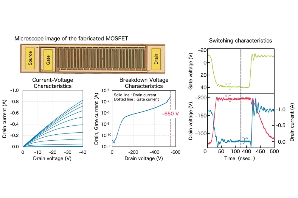
Japanese start-up Power Diamond Systems has advanced its proprietary diamond MOSFET technology and, for the first time in the world for a diamond-based device, achieved a breakdown voltage of 550 V and a drain current of 0.8 A in a single device.
Furthermore, using the same device, the company successfully demonstrated 200 V / 1 A switching operation, which it claims establishes performance at the highest level reported to date. This represents an important milestone toward the practical implementation of diamond semiconductor power devices.
The research 'Field plate multi-finger diamond MOSFET with ampere-class current capability and breakdown voltage of 550 V' was accepted for publication in Applied Physics Express on February 24, 2026, and has been published online.
Diamond semiconductors possess outstanding material properties, including a wide bandgap, an extremely high dielectric breakdown field, and exceptional thermal conductivity, making them a promising next-generation power device material that could surpass conventional semiconductors such as silicon, SiC, and GaN.
For practical implementation, however, achieving both high breakdown voltage and low on-resistance has remained a key technological challenge. In particular, from the standpoint of improving breakdown voltage, the concentration of the electric field at the gate edge has limited the drain–source breakdown voltage.
In addition, realising both high current capability and switching characteristics required for device evaluation necessitates reducing the effective area of each device and connecting a large number of small devices in parallel.
In this study, Power Diamond Systems advanced its diamond MOSFET platform technology by introducing a field-plate structure, which suppresses electric field concentration at the gate edge and enables higher breakdown voltage. At the same time, the device area was increased to enable high-current operation, thereby achieving large-current driving without relying on the parallel connection of many small devices, which had been a limitation in previous approaches.
As a result, a single diamond MOSFET successfully achieved both a device breakdown voltage of 550 V and a drain current of 0.8 A. The company says this result demonstrates the effectiveness of its device design and process technologies, including the implementation of the field-plate structure.
Furthermore, using the same device, the team achieved 200 V / 1 A switching operation, the first demonstration of such performance in a diamond MOSFET worldwide. This achievement, says the company, indicates that diamond power devices have progressed from the stage of static characteristic evaluation to verification of practical switching operation.
Power Diamond Systems has also established a stable fabrication process that enables the reproducible production of devices, demonstrating both the reliability of the technology and steady progress toward practical implementation.
Looking ahead, the company will further strengthen technology development and application development through collaboration with research institutions and industry partners in Japan and overseas, with the aim of accelerating the societal implementation of diamond semiconductor devices.
Part of this work was supported by a commissioned project from NEDO (New Energy and Industrial Technology Development Organisation) (Project No. JPNP14004) and by the “Advanced Research Infrastructure for Materials and Nanotechnology in Japan” program of the Ministry of Education, Culture, Sports, Science and Technology (MEXT).


