
Optical metrology in VCSEL processing
By drawing on optical metrology data across the entire VCSEL manufacturing process chain engineers improve their capability to target precise wavelengths and boost yield.
BY ANDRE MAAßDORF, MORITZ BRENDEL, ANDREAS RENKEWITZ, RALPH-STEPHAN UNGER AND MARKUS WEYERS FROM FERDINAND-BRAUN-INSTITUTE (FBH) AND JOHANNES ZETTLER AND KOLJA HABERLAND FROM LAYTEC
The VCSEL, a well-established class of laser that’s generating substantial sales, is enjoying success in an increasing number of applications. Most of this revenue comes from providing a light source for facial recognition in smartphones, and in datacoms, where it’s valued for its high-modulation rate.
In both these applications, the wavelength of the emission is not that critical – but that’s not the case in space applications, like highly sensitive nuclear magnetic resonance gyroscopes. Critical to the operation of these gyroscopes are single-mode lasers emitting at exactly 795 nm, a wavelength that ensures pumping and probing of a rubidium gas cell. This cell is key to sensing rotation and ensuring accurate altitude control in small CubeSats, capabilities that are not possible with today’s state-of-the-art technology.

Figure 1. Simulated white light reflectance (WLR) response in normal
incidence for the VCSEL layer sequence (a), consisting of the lower n-type doped DBR (blue layers), the cavity layers including the quantum wells (QWs, yellow) and a p-type doped top DBR (red layers). (b) Reference spectrum. (c) n-DBR layers detuned by +1 nm. (d) Upper cavity layers detuned +3 nm.
To ensure that the pump/probe configuration works, the VCSEL’s operating wavelength must be within a ±1 nm tolerance window, centred around the central wavelength of 795 nm. This requirement dictates that the VCSEL cavity resonance wavelength, also called Fabry-Pérot or FP wavelength, must be precisely within this window. Note that the FP wavelength is a result of the etalon effect – and it’s essentially defined by details surrounding the round trip that light takes inside the cavity, formed by bottom and top mirrors separated by a distance of a few hundred nanometres. So, to be able to meet demanding wavelength accuracy requirements, epitaxial engineers must fulfil a thickness accuracy requirement, and ultimately grow a stack of epilayers with sub-nanometre-precision.
Our partnership between the Ferdinand-Braun-Institute and LayTec has been considering these requirements, along with their implications. This has led us to consider this important question: what does sub-nanometre-precision actually mean, and how can we get there by using and combining the different optical metrology systems available across the production chain? In the remainder of this article we offer an answer to this key question.

Figure 2. Different metrology systems across the VCSEL production chain: (a) In-situ reflectance, temperature and curvature during growth; (b) Ex-situ WLR mapping after growth; (c) In-situ reflectance during plasma etch.
Let’s begin by illustrating the precision requirements, by looking at a simulated white-light reflectance spectrum of a typical top-emitting VCSEL layer sequence, illustrated in Figure 1. We can simulate the white-light reflectance response for the VCSEL layer sequence, considering normal incidence from the top surface.
There are two characteristic features in this response: the spectral position of the stop band centre wavelength (SBC), and the so-called FP-dip wavelength. When thicknesses within the VCSEL structure change, the SBC and the FP-dip are shifted. For example, if we increase the n-DBR period thickness by 1 nm (see Figure 1 (c)), we red-shift the FP-dip by 4 nm. Less impactful, but nonetheless similarly important, is what happens when we increase the cavity thickness above the quantum well by 3 nm (see Figure 1 (d)). With this change the FP-dip red-shifts by only about 1 nm. These results make the point that to ensure a FP-dip sits well inside the ±1 nm target window, the layer thicknesses in the DBRs must be grown with sub-nanometre precision.

Figure 3. In-situ growth rate determination from reflectance transients: (left) Schematic layer sequence showing a two-layer stack on a silicon-doped GaAs substrate; (right) oscillating 950 nm reflectance transient (symbols), with the oscillations caused by the layer thickness steadily increasing during epitaxial growth.
So far, we have focused on precision requirements. Now let’s delve into the implications, considering the case of growing the VCSEL structure shown in Figure 1 by MOCVD. According to our experience, we can expect the precision associated with growth rates to usually be in range of ±1 percent. Imagine we want to grow a 6000 nm-thick GaAs layer. Based on knowledge of the growth rate from a previous, sufficiently recent growth process, we will be able to grow a GaAs layer with a thickness of around (6000 ± 60) nm. For a VCSEL with a total thickness of 6 µm and a distributed Bragg reflector with around 60 periods in total, each period would be off by 1 nm at worst.
Unfortunately, our simulations show that a 1 nm detuning in thickness for just the n-DBR periods produces a 4 nm detuning in the FP-dip (Figure 1 (c)). So, we must have a growth rate accuracy that’s far better than ±1 percent. We accomplish this challenging requirement by heavily relying on optical metrology during (in-situ) and after (ex-situ) the growth process.
Combining metrology systems
We have several optical metrology systems employed for our VCSEL fabrication process (see Figure 2). One of these systems gathers in-situ reflectance data during growth (see Figure 2 (a)). We have tracked the 950 nm transient during the growth of two layers that subsequently provide the quarter-wave layers in the superlattice periods that form the DBRs in our VCSELs: Al0.22Ga0.78As and Al0.90Ga0.10As.

Figure 4. White-light reflectance mapping providing a full spectrum (bottom right) at each position on the wafer.
Information buried within the Fabry-Pérot oscillations of the reflectance profile reveals the speed each layer thickness is increasing. By using a virtual interface approach to model these oscillations, we calculate this speed, usually referred to as the growth rate. Values for two determined growth rates are provided at the top in the viewgraph on the right in Figure 3.
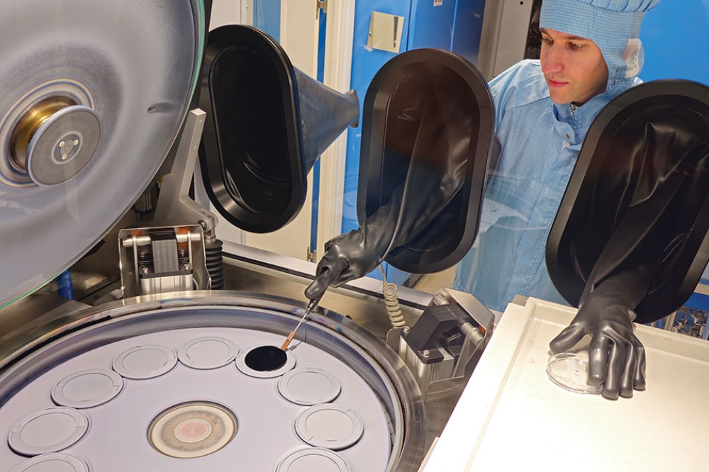
Within Figure 2, also shown is the ex-situ WLR mapping instrument – it’s part (b). Used after epitaxial growth, this tool records the optical response at each position on the wafer, following illumination with white light at normal incidence (see Figure 4).
Calibration scheme
Our WLR mapping data is incredibly useful. As well as helping to evaluate and optimise the homogeneity of the SBC and FP-dip, it plays an important role in our calibration scheme, which begins with the growth of a shorter version of the full VCSEL layer sequence. For this trimmed-down epistructure, the number of superlattice periods for both the top and the bottom DBR is decreased to just 10 periods (see the right of Figure 5).
This alteration trims the epitaxial growth time from 6 hours or so to less than 3 hours, while maintaining the strong features in the WLR spectrum (see the left of Figure 5).
We use the measured WLR spectrum to fit the modelled counterpart, varying the DBR period thicknesses for top and bottom DBRs individually, as well as the cavity thickness. With this method we are unable to accurately determine the two quarter-wave layer thicknesses individually, as they are not represented by a strong feature in the WLR spectrum. Due to this limitation, we draw on previous values for growth rates (see Figure 3).
This involves assuming that the ratio of the two quarter-wave layers is equal to the ratio of the two growth rates – it is a reasonable claim, so long as we use exactly same growth conditions for the two-layer sample described in Figure 3, and the DBR layers in the shortened VCSEL layer sequence, detailed in Figure 5.

Figure 5. Measured (dashed) and modelled (solid) WLR spectra of the shortened VCSEL layer sequence, as shown in the schematic on the right.
Using this fitting to the model, we have determined cavity and DBR thicknesses. In the example we are sharing, the SBC and FP-dip wavelengths are about 3 nm above the target wavelength of 795 nm. So, we change the model parameters, adjusting the DBR thicknesses by -0.5 nm, equally distributed across the two quarter-wave layers, as well as the cavity thickness by -3.2 nm, also equally distributed across the individual layers around the quantum wells. We obtained these values by gradual adjustment and simulation, closing in until the simulated spectral profile is exactly centred around the target wavelength.
Following this, we applied changes to the growth recipe, along with an increase in the number of repeats for top and bottom DBRs, to 21 and 41, respectively. The measured WLR spectrum of this full VCSEL structure is nicely centred around the target wavelength (see Figure 6).
This completes the procedure that we use to nail the target wavelength for one wafer.
In-situ feed-forward
As our MOCVD has the capacity to accommodate 12 wafers in one process, we must ensure that all the wafers are on target.
We have shown that we can accomplish this goal. This is possible because reflectance data is measured for each wafer individually. Figure 7 (a) shows the colour-coded reflectance data for one wafer as an example. In these kinds of plots, wavelength-resolved reflectance is represented by horizontal lines, stacked along the vertical time axis to provide transient information for those spectra. Inspection of these plots reveals unique signatures during n-DBR, cavity and p-DBR growth. Analysing these signatures in real-time yields transient data lines (see Figure 7 (b)) for the SBC (solid) and the FP-dip (dashed) for each wafer.

Figure 6. Measured (dashed) and modelled (solid) WLR spectra of the
full VCSEL layer sequence, shown in the schematic on the right, with the
delta changes applied to the growth recipe, as determined from the
model in Figure 5.
Based on in-situ analysis (not shown) of the shortened VCSEL growth as part of the calibration scheme explained earlier, we know the target wavelengths for SBC and FP-dip at the growth temperature (this is indicated by the blue and green dashed lines in Figure 7 (b)). Due to a technical limitation of our metrology set-up, we are only able to monitor 9 of the 12 wafers with full spectral transient analysis. Now, if any of the SBC transients of our wafers is offset from this target during n-DBR growth, we can make online adjustments. The changes provide corrections to the subsequently grown layers and the FP-dip, with success revealed once the p-DBR starts growing.
To carry out our online adjustments, we make use of the so-called gas-foil rotation (GFR). Within our MOCVD system, there are 12 graphite wafer carriers – also known as satellites – all put into rotation by hydrogen gas, spirally flowing in a gap below the carrier, from the centre to the outside. As well as causing the carrier to rotate, the spiral motion of the gas produces partial mixing and dilution of the main process gasses flowing on top of the carrier across the wafer. This dilution slightly affects growth rate. That can be to our advantage, as by varying the GFR flow rate, we can fine-tune the growth rate.

Figure 7. In-situ feed-forward procedure based on spectral WLR VCSEL
analysis during growth and per-satellite adjustment of the gas-foil
rotation flow rate in order to homogenize the wafer to wafer spread for
SBC and FP-dip.
The benefits of individual GFR flow rates are evident in Figure 7 (b), which includes GFR profiles (top right). By comparing the SBC spread during n-DBR growth, and before and during p-DBR growth, one can see that by applying adjustments to the GFR flow rates during growth of the n-DBR, we decrease the spread from ±8 nm to ±2 nm – that’s a significant improvement.
Another opportunity that’s open to us is to draw on the full reflectance transient recorded during growth of the VCSEL layer sequence (see Figure 6), and undertake a full-stack simulation and fit. This exercise allows us to determine all the layer stack parameters. The result of this model fit is shown in Figure 8. You can see that the fit provides a good representation of the measured transient. One can benefit from this knowledge when undertaking front-end processes on the grown wafers.

Figure 8. Measured (grey) and simulated (blue) 488 nm reflectance transient during growth of the VCSEL layer sequence already shown in Figure 6.
Connecting growth and etch
One of the critical steps in VCSEL processing is the formation of a mesa, defined by etching down to the bottom DBR and precisely stopping below the active region. This step takes place before forming a current aperture by wet oxidation of a layer with high aluminium content. Again, optical in-situ metrology is used to monitor and control the plasma etching process.
Based on full-stack simulation, we can use that layer stack, remove all growth interruptions and calculate the transient in the reverse direction – now starting at the surface and progressing towards the substrate. Similarly, we can do the same with the layer stack obtained with WLR analysis (see Figure 6), and calculate an expected transient.
Shown in Figure 9 is a comparison of two predicted 488 nm transients. One is from the in-situ transient analysis (Figure 8); and the other from ex-situ WLR analysis in Figure 6, shown together with the actually measured 488 nm transient during plasma etch of the VCSEL mesa.

Figure 9. Measured (grey symbols) and modelled 488 nm transients
during plasma etch of the VCSEL layer sequence shown in Figure 8.
As you can see, both approaches produce a reasonably good agreement with the measured etch transient. The implication is that by using the knowledge gathered during epitaxial growth, it’s possible to implement feature-based end-pointing in plasma etching. For non-periodic layer sequences, such as those found in edge-emitting lasers, this approach is even more powerful, as there are far fewer interfaces from which one could deduce the approximate depth. Note also that for these non-VCSEL-like structures, such as the layer structures found in edge-emitting lasers and devices with similar layer sequences, the WLR profile tends to be devoid of any strong features. Due to this, the only viable way to deduce the layer stack parameters is full-stack transient reflectance analysis (see Figure 8). Thus, this connected way of utilising metrology is currently expanded to non-VCSEL-like structures.


