
Taking GaN in a different direction
Infineon has just released a pair of bi-directional switches for mobile applications that block up to 40 V.
BY RICHARD STEVENSON, EDITOR, CS MAGAZINE
For many makers of GaN power devices, much effort is directed at increasing their blocking voltage from around 600 V to 1 kV and beyond. By entering territory that’s occupied by SiC MOSFETs, there’s the opportunity to compete for sales to the electric vehicle industry and to installers of electrical grid infrastructure. But there is also the promise of ramping revenues by launching products operating at much lower voltages, which can be deployed in mobile devices – note that here, it is also possible to exploit the strengths of GaN, such as high switching frequencies, excellent efficiencies and impressive power densities.
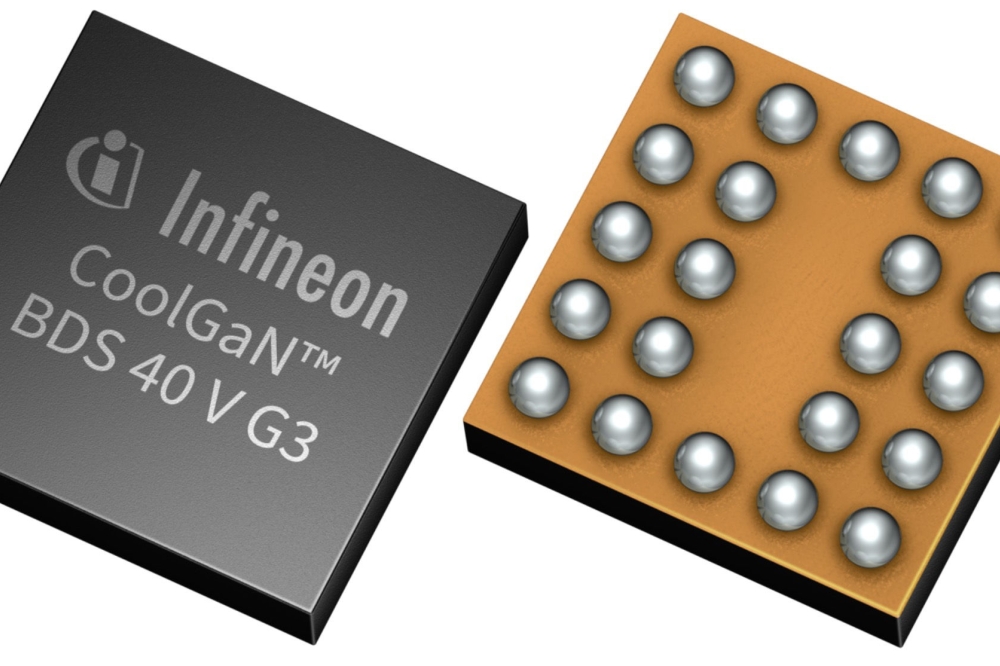
One company seeking success on the latter front is Infineon. This multi-national launched its first 40 V bi-directional switch last summer, and based on its reception, has just expanded the portfolio with two more products providing the same blocking voltage: the IGK048B041S and IGK120B041S. This duo differs in size – they have dimensions of 2.1 mm by 2.1 mm², and 1.7 mm by 1.2 mm² – and in drain-to-drain on resistances, which are 4.2 mΩ and 9 mΩ, respectively.
A key asset of Infineon’s switches, giving them an edge over the incumbent silicon solution (a pair of MOSFETs), is their bi-directionality. This means that they can conduct in both directions, and also block up to 40 V in both directions.

Given the relatively
thin GaN epilayers in 40 V bi-directional switches, these products are
strong contenders for volume production on 300 mm lines.
A collaborative development
For the development of Infineon’s first product, the company collaborated closely with a smartphone manufacturer.
“For us, this was also co-developing, learning, understanding the value proposition,” reveals Infineon’s Senior VP and General Manager of the GaN Business Line, Johannes Schoiswohl. He told Compound Semiconductor that they drew on what they had learnt from the launch of the first switch when introducing the two new products, a move that offer customers different values for the likes of resistance and impedance.
Given that smartphone batteries provide just a few volts, deploying devices with a blocking voltage of 40 V suggests excessive over-engineering. But that view overlooks that fast charging a mobile a via USB-C cable may involve voltages of 20 V or 28 V. It’s also possible that when plugging and unplugging cables, voltage spikes may occur, which must be protected from the battery. “So there needs to be enough headroom. That's why it's a 40-volt device,” says Schoiswohl.
As well as targeting mobile phones, Infineon is eyeing opportunities in wearables, such as smartwatches, fitness trackers, augmented-reality glasses, wireless earbuds, and smart rings. For all these products, high-power charging is attractive.
Inside every Infineon 40 V bidirectional switch is a pair of HEMTs, united monolithically. Employing a common source or drain ensures bi-directionality, along with control of the current flow and blocking behaviour.
Using these small switches as alternatives to pairs of silicon MOSFETs, arranged in a back-to-back configuration, halves component count and trims the footprint by up to 82 percent.
Another advantage over the silicon MOSFETs is a reduction in gate charge by 40 percent.
“So, essentially you can say it turns off with double speed, versus a silicon switch,” says Schoiswohl, who explains that superior protection results.
Offering yet another advantage over silicon technology is the minimal drain-to-drain leakage current – it is 85 percent lower. That’s a very attractive feature for makers of smartphones that will charge the batteries to a certain level before shipping. It’s imperative that their smartphones, which could sit on the shelves of stores for many weeks, will turn on when shoppers compare various models.
As well as improving the performance of mobile devices, Infineon’s bidirectional switches can help fulfil safety requirements, needed to reduce the likelihood of electrical fires from lithium-ion batteries. There is much documentation to support an ever-growing number of stringent safety requirements, including a need for higher overvoltage protection. The 40 V bi-directional switch addresses these specifications.
Thanks to the 40 V capability, Infineon’s switches are also ideal for load-switching and power multiplexing in multi-rail power architectures, where there’s a need for precise control of current direction across multiple supply rails. This situation is a common one, as the electronics within a smartphone may run off of a 5 V rail, and fast-charging may operate at 20 V or 28 V.
Scaling production
Production of Infineon’s switches is not particularly complicated, according to Schoiswohl: “It's just a different layout, versus the unidirectional switch.”
Today, the company makes its bidirectional switches on 200 mm lines. “But the target is to be in mass production by end of next year on 300 millimetre.”
A downside of moving to the larger format is that it exacerbates issues associated with wafer bow, stemming from lattice and thermal mismatches between GaN and silicon. But within Infineon’s GaN portfolio, the 40 V devices should be relatively easy to move to the 300 mm line, given the relatively thin GaN layers required to block 40 V.
On the plus side, there is much to motivate a move to the bigger wafers. “Because the tools are so advanced, that makes it really tempting to move as fast as possible to 300 millimetre, especially for us, because we can reuse 80 percent of our silicon 300 millimetre lines.”
When Infineon ramps production, the handset will yet again provide a major market for a compound semiconductor device. While smartphones no longer account for significant sales of LEDs, they still provide much business for makers of GaAs RF devices, and they now look to offer a significant revenue stream for some producers of GaN power electronics.


