

KAIST-led team develops next gen ALD process
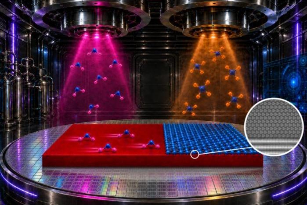
A research team from the Korean Advanced Institute of Science and Technology (KAIST) led by Joonki Suh from the Department of Chemical and Biomolecular Engineering, in collaboration with Bonggeun Shong's team at Hanyang University and Yimo Han's team at Rice University in the US, has developed a new semiconductor manufacturing technique based on atomic layer deposition (ALD).
The study 'Van der Waals template-encoded soft epitaxy of tellurium enabled by atomic layer depositions' was published in the journal Science Advances on July 24 2026.
The scientits focused on van der Waals materials - 2D semiconductor materials consist of multiple atomic layers held together by weak interlayer forces. Because different materials can be freely stacked, van der Waals materials are attracting attention as key building blocks for next-generation AI chips and ultra-low-power semiconductor devices.
However, their chemically stable surfaces make it difficult to grow new semiconductor layers in a uniformly aligned orientation. This challenge becomes even greater at lower temperatures, where atoms tend to nucleate and grow in random directions, making it difficult to produce high-performance semiconductor films.
The research team developed a new method that allows tellurium (Te)-containing precursors—molecular building blocks used to fabricate semiconductors—to move freely across the surface, find the most energetically stable positions, and form a thin film.
Tellurium is attracting attention as a key material for next-generation semiconductors and optoelectronic devices, including photodetectors and LEDs, because it combines highly direction-dependent electrical conductivity with excellent light-controlling properties.
Using this approach, the research team succeeded in achieving epitaxial growth of tellurium uniformly in a single direction on van der Waals materials at a low temperature of 150°C using ALD.
The researchers also confirmed that the technology could be applied to a range of van der Waals materials, including WSe2, MoS2, ReSe2, and mica.
The team further used the resulting semiconductor films to fabricate transistors as well as optoelectronic devices that detect or emit light.
"This study is the first to demonstrate that high-quality semiconductor films can be grown on van der Waals materials at low temperature without damaging the underlying materials," said Suh. "We expect this technology to serve as a key manufacturing platform for integrating a wide range of next-generation semiconductors on a single chip," he added.



