
Sputtering superior ohmic contacts
A collaboration between researchers in Singapore and Japan has developed a sputtering technology for ohmic contacts that aids the performance of GaN HEMTs. The team argues that its approach, an attractive alternative to producing ohmic GaN contacts by MOCVD and MBE, improves the prospects for GaN HEMTs in mobile applications.
If GaN HEMTs are to be deployed in handsets and mobile infrastructure, they need to operate at around 3.3 V and 8-12 V, respectively. For these voltages, a low ohmic contact resistance is essential.
Realising this requirement is the collaboration’s sputtering technology, developed by researchers from: Nanyang Technical University, Singapore; Singapore’s National Semiconductor Translation and Innovation Centre for Gallium Nitride; and Nagoya University, Japan.
One of the strengths of sputtering is its lower growth temperature, according to corresponding author Geok Ing Ng, who holds positions at both Nanyang Technical University and the National Semiconductor Translation and Innovation Centre for Gallium Nitride.
According to Ng, at around 600 °C, and possibly at even lower temperatures, sputtering produces n-GaN with reasonable crystalline quality. In comparison, producing n-doped GaN by MBE and MOCVD requires growth temperatures of typically around 750 °C and beyond 900 °C, respectively. “Such high temperatures typically necessitate the use of an ohmic-first process, which limits process flexibility.”
Another advantage of sputtering is its widespread tool availability. Today’s CMOS foundries tend to have sputtering tools, but not those for growth by MBE and MOCVD. “These sputtering tools, though configured for the CMOS process, could be readily modified to support GaN sputtering,” says Ng.
The team are not the first to consider sputtering n-type GaN, with previous efforts forming highly doped n-GaN ohmic contacts on GaN HEMT heterostructures
“To the best of our knowledge, this work is the first report of ohmic contact to an InAlN/GaN heterostructure, which is a strong contender for high-frequency, low-voltage GaN HEMTs,” says Ng.
According to him, another breakthrough is the successful integration of sputtered ohmic contacts for scaled gate length GaN HEMTs.
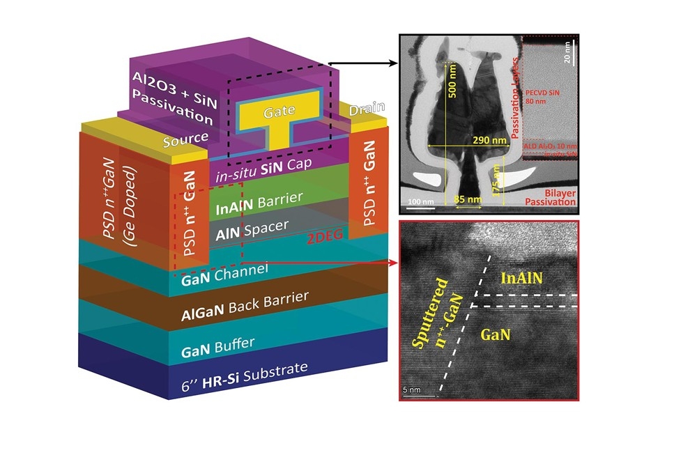
Critical to success, says Ng, is ensuring a good fill of sputtered GaN, and high-quality patterning in the closely spaced source-drain regions. Engineers also had to make sure they did not damage the SiN cap, which is just 2 nm-thick.
Fabrication of the HEMTs began by loading high-resistivity silicon substrates into an MOCVD chamber and adding a carbon-doped GaN buffer, a 250 nm-thick AlGaN back barrier, an 80 nm-thick GaN channel, a 2 nm-thick AlN spacer, a 7 nm-thick InAlN barrier and a SiN cap.
From this epiwafer the team produced GaN HEMTs with a source-to-drain distance of 2.5 µm and a gate length of 85 nm. To form the ohmic contact, reactive ion etching recessed this region by 50 nm, before a radical-enhanced reactive sputtering systems added 80 nm-thick germanium-doped GaN at 600 °C, at a rate of 6.3 nm min-1. The sputtered GaN is initially crystalline, and then polycrystalline, with the latter removed with a TMAH etch.
Characterisation determined an interfacial resistance between the n-type GaN and the two-dimensional electron gas of 0.06 Ω mm and an on-resistance of 0.91Ω mm. The HEMT produces a maximum drain current of 2.03 A mm-1, and output powers at 28 GHz of 0.51 W mm-1, 1.25 W mm-1 and 2.44 W mm-1, at drain-source voltages of 3 V, 5 V and 8 V, respectively.
One of the next goals for the team is to see if they can obtain a lower contact resistance. “Secondly, we plan to implement sputtered GaN ohmic contacts in our improved low-voltage transistors with aggressive scaling, to explore the performance limits of these transistors,” says Ng.
Pictured above: InAlN/GaN HEMTs with a T-shaped gate and sputtered regrown n-type contacts, imaged with a scanning electron microscope.
Reference
Y. Zhuang et al. Electron Dev. Lett. (early access)


