

Efficacious excitation aids n-type AlN
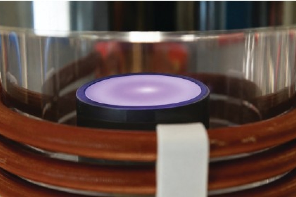
Illuminating the MOCVD chamber with a source that emits deep within the UV boosts the mobility of silicon-doped AlN and its free-electron concentration.
BY FIKADU ALEMA, WILLIAM BRAND, VITALI SOUKHOVEEV, AARON FINE AND ANDREI OSINSKY FROM AGNITRON TECHNOLOGY
Within the family of ultra-wide-bandgap semiconductors, AlN has much appeal. Its strengths include a bandgap of around 6.2 eV, a critical breakdown field that exceeds 15 MV cm-1, and a thermal conductivity of almost 340 W m-1 K-1. What’s more, native substrates are commercially available, giving AlN a route to low-defect-density epitaxy that’s not available for every emerging wide-bandgap material. Thanks to all these attributes, AlN is an incredibly attractive candidate for next-generation power electronics and deep-ultraviolet optoelectronics.
However, there’s a critical issue: realising conductive, n-type AlN layers with sufficient free-electron concentrations and adequate mobility. Simply injecting more silicon, the most common donor in III-nitrides, is not a solution. While high levels of silicon are effective in GaN and gallium-rich AlGaN, where this impurity behaves as a shallow donor, in AlN silicon activation is far less efficient. Adding this donor creates a number of imperfections, including silicon-related DX centres, aluminium vacancies, vacancy-silicon complexes and background impurities – all can trap or compensate electrons. While increases in silicon doping initially produce a rise in free-electron concentration, mobility often collapses, with compensation eventually limiting further improvement [1-3].
Recently, our team at Agnitron has refined the MOCVD process to attack this problem from two directions. One is chemical potential control – using growth pressure, temperature, V/III ratio and precursor delivery to influence point defect formation during growth. And our second direction is defect quasi-Fermi-level control, realised by using above-bandgap illumination to alter the carrier population and suppress the formation of compensating defects during the epitaxial process [4, 5].
In the pages of this publication we previously reported how these strategies hold much promise for the growth of high-quality silicon-doped AlN and aluminium-rich AlGaN [6, 7]. Now we are adding another control knob: deuterium vacuum-ultraviolet (D₂-VUV) illumination during growth of silicon-doped AlN by MOCVD.
Influencing defect formation
During defect quasi-Fermi-level control, we control the incorporation of point defects with UV-assisted epitaxy. This involves using a source of above-bandgap photons to generate carriers near the growth surface that shift quasi-Fermi levels and change the formation energies of charged point defects. Under these conditions, it’s possible to reduce the incorporation of compensating defects in AlN, and increase the fraction of silicon donors that contribute free electrons.
Note that this approach is strongly material dependent. UV sources that work well for GaN may fail to provide photons with enough energy for AlN, which has a much larger bandgap and requires much shorter wavelengths. For this reason, spectral matching is critical. For growth of AlN, mercury-xenon lamps, which emit strongly across many UV wavelengths and have been useful in III-nitride growth studies, are not ideal – much of their output is at wavelengths too long to efficiently excite AlN under growth conditions. Far better are D₂-VUV sources, which provide strong emission near 160 nm and deliver higher-energy photons that interact more effectively with the growing AlN surface (see Figure 1).

Figure 1. Spectral comparison of the mercury-xenon lamp (a) and the deuterium vacuum-ultraviolet source (b) used for UV-assisted MOCVD. The D₂-VUV source provides stronger short-wavelength emission near 160 nm, making it a better match for above-bandgap excitation of AlN than the Hg-Xe lamp.
Initially, we evaluated UV-assisted growth using a mercury-xenon source. Investigations involved growth on Crystal IS AlN substrates in an Agnitron Agilis 100 MOCVD reactor equipped with a remote-injection showerhead. Trimethylaluminium, ammonia and silane provided the aluminium, nitrogen and silicon precursors, respectively. To isolate the effect of UV exposure, we grew pairs of silicon-doped AlN layers under identical process conditions. For UV-assisted samples, we only switched the Hg-Xe lamp on during growth of the silicon-doped AlN layer.
Measurements of our samples showed that ultraviolet exposure influences AlN growth. However, benefits are limited with the mercury-xenon source. Using this form of UV illumination, the free-electron concentration increased from about 8 × 10¹⁴ cm-3 to 1.5 × 10¹⁵ cm-3, electron mobility fell from around 107 cm² V-1 s-1 to roughly 90 cm² V-1 s-1, and bulk resistivity fell from about 73 Ω cm to around 49 Ω cm.
Secondary-ion mass spectrometry (SIMS) offered valuable insight into these changes. Under Hg-Xe exposure, silicon incorporation increased from approximately 6.5 × 10¹⁷ cm-3 to 7.7 × 10¹⁷ cm-3 – that’s a rise of about 19 percent. Meanwhile, carbon and oxygen concentrations remained essentially unchanged. These results suggest that donor activation efficiency increased slightly, from roughly 0.15 percent without UV exposure to about 0.20 percent with Hg-Xe exposure. We concluded from these findings that Hg-Xe illumination measurably affects silicon-doped AlN growth, primarily by increasing silicon incorporation and carrier concentration, but these are only small gains in donor activation, highlighting insufficient spectral matching between the UV source and the material.
Due to this limitation, we integrated a D₂-VUV source into our Agilis 100 MOCVD reactor. With strong emission deep within the UV, this source provides a better spectral match to AlN, and ensures more effective above-bandgap excitation during growth.
We direct the VUV light at the growing surface via a custom remote-injection showerhead with a central optical-access region. With this design, our compact D₂-VUV source is mounted directly above the reactor and optically coupled to the growth surface. Ammonia is introduced through the central region, and metalorganic precursors delivered through an annular region surrounding the optical access.
With D₂-VUV exposure, there’s a similar increase in silicon incorporation to the Hg-Xe lamp, but a much larger electrical payoff. According to SIMS, silicon concentration increases from about 4.2 x 10¹⁷ cm-3 to roughly 5.0 × 10¹⁷ cm-3 with D₂-VUV exposure, corresponding to an increase of about 19 percent (see Figure 2). The concentration of carbon remains near the SIMS detection limit, while oxygen decreases through the film, and does not show dependence on the UV exposure.

Figure 2. Secondary-ion mass spectrometry (SIMS) analysis of silicon-doped AlN grown on a Crystal IS AlN substrate with and without D₂-VUV exposure. (a) SIMS test structure. (b) Depth profiles of silicon, oxygen and carbon. (c) Linear-scale silicon profile showing an approximately 19 percent increase in silicon incorporation under D₂-VUV exposure.
Another important observation is that the illumination of the surface with UV reduces the growth rate. Our view is that the increase in silicon concentration under UV exposure may be partly linked to growth-rate-mediated surface kinetics: a slower AlN deposition increases the effective residence time of silicon-containing species at the growth surface, enhancing their probability of incorporation.
When conducting additional growth-rate experiments on AlN/sapphire templates, we uncovered a striking trend. Without UV, the growth rate increases with V/III ratio in the custom showerhead. But with D2-VUV exposure, this relationship reverses, with growth rate decreasing as V/III ratio increases. This shows that VUV illumination should not be thought of as the addition of passive light to an otherwise unchanged MOCVD process – rather, D₂-VUV illumination is part of the growth chemistry, probably altering ammonia photodissociation, gas-phase precursor reactions, surface reaction pathways, or some combination of these effects. While the detailed mechanism requires further study, it’s clear that VUV illumination changes how AlN grows.
Breaking trade-offs
With D₂-VUV-assisted growth, the overwhelming advantage is the superior trade-off between mobility and carrier concentration in silicon-doped AlN. Using this technology, AlN now has a high enough carrier concentration to reduce resistance, while retaining sufficient mobility to avoid the severe transport penalty normally associated with heavy compensation.
Measurements reveal that with the introduction of D₂-VUV exposure, electron mobilities increase from 20-110 cm² V-1 s-1 to 100-160 cm² V-1 s-1, and free-electron concentration climbs from 6 x 10¹⁵ cm-3 to 1 x 10¹⁶ cm-3 (see Figure 3, left). One of our best results – highlighting our breakthrough – is a free-electron concentration of about 3 × 10¹⁶ cm-3, combined with an electron mobility of about 80 cm² V-1 s-1
Another important characteristic is resistivity. Several of our D₂-VUV-grown AlN samples have values below 10 Ω cm, with the best film reaching a bulk resistivity of about 2.7 Ω cm (see Figure 3). This value, which is lower than previously reported bulk resistivities for MOCVD-grown silicon-doped AlN, showcases the significant improvement in the conductivity of AlN grown by MOCVD [2].

Figure 3. Electrical performance of silicon-doped AlN grown on Crystal IS substrates. Electron mobility (left) and bulk resistivity (right) are plotted as functions of Hall-measured free-electron concentration. D₂-VUV-assisted growth extends the free-electron concentration above the non-UV range while preserving useful mobility, and it shifts the films into a lower-resistivity regime. The best sample combines a free-electron concentration of 3 x 10¹⁶ cm-3 with a mobility of around 80 cm² V-1 s-1, giving resistivity of 2.7 Ω cm.
Record activation efficiencies
To estimate the donor activation efficiency of our most conductive D₂-VUV-grown film, we have compared the Hall-measured free-electron concentration with the SIMS-measured silicon concentration. For the sample with a free-electron concentration of approximately 3 × 10¹⁶ cm-3, the silicon concentration is about 1.3 × 10¹⁷ cm-3, implying a donor activation efficiency of roughly 22 percent. That’s a very impressive figure – it’s more than 100 times higher than the value estimated for the Hg-Xe-exposed film, and nearly two orders of magnitude higher than typical values reported for MOCVD-grown silicon-doped AlN.
A careful look at our SIMS results uncovers an important clue concerning the mechanism associated with D₂-VUV exposure. As there’s no reduction in carbon or oxygen incorporation, it’s unlikely that the dramatic improvement in conductivity results from lower impurity levels. Instead, the results point to improved donor activation and reduced compensation by point defects during growth. Since VUV exposure changes the growth-rate behaviour, we have deduced that the most likely cause of overall improvement is a combination of modified growth chemistry and defect quasi-Fermi-level control.
We have also investigated whether D₂-VUV-assisted MOCVD aids the growth of high-aluminium-content AlGaN. Using D₂-VUV exposure, we produced Al0.87Ga0.13N that is conductive, and has Hall-measured electron concentrations reaching 3.1 x 1019 cm-3. Specific contact resistivity reaches up to 7.5 x 10⁻⁵ Ω cm², compared with 1.7 x 10⁻⁴ Ω cm² for a comparable layer grown without D₂-VUV exposure. That corresponds to a reduction in specific contact resistivity of approximately 57 percent. Based on these results, the benefits of D₂-VUV illumination are not limited to binary AlN – they support improved conductivity and contact behaviour in high-aluminium-content AlGaN.


Deep UV exposure capability
Playing a key role in the success of our recent UV-assisted AlN work is the Agilis 100, our most widely adopted OEM R&D MOCVD platform. This flexible reactor is a highly configurable research tool, supporting both remote-injection showerhead and close-injection showerhead operation – this allows researchers to select the reactor geometry best suited to their material system and growth objectives. Thanks to this flexibility, our platform is particularly useful for wide-bandgap and ultra-wide-bandgap materials research, where growth chemistry, precursor delivery, thermal environment, and in-situ process control often need to be adapted as science evolves.
For the UV-assisted AlN results presented in this article, we employed a newly engineered showerhead/gas distribution flange that integrates a high-power D₂-VUV source directly into the reactor. Rather than relying on an external lamp, viewport coupling, or a long optical light pipe, by adopting this approach VUV exposure is delivered directly to the wafer carrier and growth surface. That’s valuable, as it allows the photon flux to interact with the growth environment where it is needed most, while only infringing minimally on gas delivery, to ensure high-quality growth by MOCVD.
Our development of integrated D₂-VUV hardware reflects our broader approach to reactor design: using an MOCVD platform as not only a growth tool, but an adaptable experimental environment for testing new process physics. By integrating the UV source into the showerhead region, we have created a practical path for above-bandgap exposure during the growth of ultra-wide-bandgap materials, such as AlN.

Figure 7. Thickness uniformity map of a Ga₂O₃ film grown on a 4-inch sapphire substrate in the Agilis 700 using Dynamic Sweep Gas Modulation. The sweep-modulated growth achieved approximately 1 percent 1σ thickness non-uniformity.
Dynamic sweep gas modulation
Another recent breakthrough is our demonstration of a new uniformity-control approach on our larger-format Agilis 700 platform – this is one of our most capable MOCVD systems for developing advanced oxides, including β-Ga₂O₃ and related materials. On platforms supporting larger wafers, it is critical to maintain uniformity across larger substrates. Building on observations made during the development of our horizontal AgniGaN 400 reactor, we have developed Dynamic Sweep Gas Modulation technology. This patent-pending technology (US Patent Application No. 19/715,791) actively tunes the spatial distribution of precursor flux during growth.
To realise this, we modulate selected push-gas or injection-zone flows during a growth step, rather than holding them at fixed values. Modulation may be defined through recipe parameters, such as baseline flow, amplitude, frequency, phase, duty cycle and waveform shape. By selecting fixed high-flow and low-flow conditions, process engineers may bias deposition toward different regions of the wafer or carrier. Using dynamical sweeping of the gas flow during growth, our reactor time-averages these spatial biases to produce a more uniform film. Adopting this approach in our horizontal reactor reduced the 1σ thickness non-uniformity of AlN grown on 4-inch sapphire from about 2.5 percent to approximately 0.5 percent.
Recent work with our Agilis 700 shows that we can apply the same concept to a vertical reactor configuration. In one of our sets of experiments, we compared two fixed alkyl/metalorganic-zone flow conditions, 1500 sccm and 500 sccm, with a third condition using Dynamic Sweep Gas Modulation. Fixed-flow conditions produced distinct spatial deposition profiles, while the sweep-modulated condition significantly improved uniformity, reaching approximately 1 percent 1σ non-uniformity on a 4-inch substrate (see Figure 7). These results show that Dynamic Sweep Gas Modulation is not limited to horizontal flow reactors – it can also improve vertical MOCVD platforms where gas distribution, wafer rotation, precursor utilisation and wafer-scale uniformity are tightly coupled. These improvements to uniformity, alongside advances in silicon-doping with sources deep within the UV, strengthen our position as a pioneer of high-quality ultra-wide-bandgap epilayers.
This work was supported by the Defense Advanced Research Projects Agency (DARPA) under Contract No. 140D0424C0048 (Dr. David Meyer) and by the Office of Naval Research (ONR) through the SBIR Phase II programme under Contract No. N6833520C0105 (Mr. LJP). The work on Ga2O3 was supported by a Direct to phase II SBIR project funded through AFRL under contract No. FA239423CB010 (programme monitor Dr. Adam Neal). The views, opinions, and/or findings expressed are those of the author and should not be interpreted as representing the official views or policies of the Department of War or the U.S. Government. Agnitron also acknowledges Prof. Houqing Fu of Arizona State University for collaboration on the electrical characterisation of AlGaN and AlN layers, Prof. Travis Anderson of the University of Florida for Hall measurements that confirmed the electrical data.



