

Transferable thin‑film GaN LEDs
Electrochemical etching lifts membranes of III‑nitride LEDs, opening the door to scalable integration into CMOS-based photonics.
BY MIKOŁAJ CHLIPAŁA AND HENRYK TURSKI FROM THE INSTITUTE OF
HIGH PRESSURE PHYSICS OF THE POLISH ACADEMY OF SCIENCES
Generation of visible light has been transformed by GaN. From solid‑state lighting to backlighting displays, optical communication and sensing, GaN‑based devices are deeply embedded in today’s technology. Yet as optoelectronic systems become more complex, another key requirement is coming sharply into focus: the ability to integrate high‑quality light sources onto CMOS-compatible substrates.
This particular task is far from trivial. The trait that ensures the success of GaN devices – their excellent quality when grown on native bulk GaN substrates – has a downside, as it makes them stubbornly difficult to integrate with other technologies. And as well as being technically demanding, GaN substrates are expensive, reinforcing the need to use the material as efficiently as possible.
Moreover, bulk GaN is poorly suited for integration with with photonic integrated circuits, silicon electronics and flexible electronic platforms. All three of these technologies demand substrates that are inexpensive, available in large sizes and supported by mature fabrication ecosystems – criteria that bulk GaN fails to fulfil. And one potential solution, substrate re-use, is not easy. For GaN devices grown homoepitaxially on bulk substrates, it’s been a formidable challenge to detach the active device without damaging it.

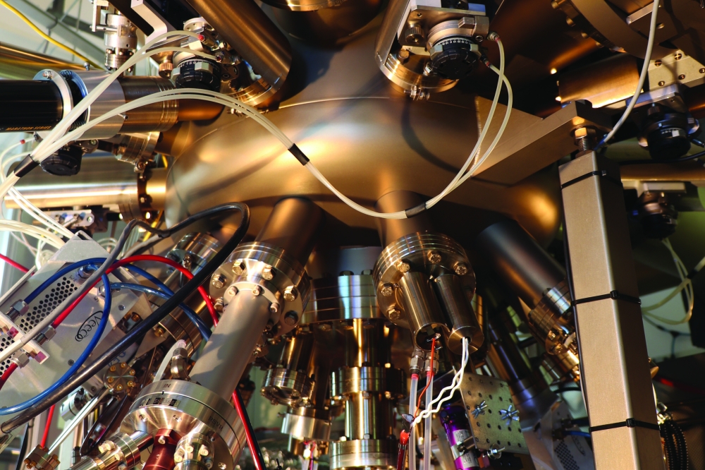
Figure 1. A plasma‑assisted MBE system at Institute of High Pressure Polish Academy of Science used for GaN LED growth. Gallium and other group‑III elements are supplied from thermal evaporation sources, while active nitrogen is provided by a radio‑frequency plasma source, enabling low‑temperature growth of high‑quality III‑nitride epitaxial layers. Photo Dr. Grzegorz Muzioł.
The good news is that a promising solution is emerging, thanks to our efforts at the Institute of High Pressure Physics of the Polish Academy of Sciences. By combining epitaxial design with low‑voltage electrochemical etching, we cleanly release ultra‑thin GaN LED membranes, incorporating nanometre‑smooth back surfaces. From there we integrate these membranes on foreign substrates by micro‑transfer printing, while retaining electrical and optical performance. This approach provides a practical pathway to heterogeneous integration of high‑quality GaN light sources, accomplished without sacrificing the exceptional strengths of these emitters.
The value of native substrates
For the growth of GaN LEDs, a native substrate is superior to both sapphire and silicon, as it enables a significantly lower threading dislocation density. Thanks to this, devices have higher current handling, higher efficiency, enhanced reliability and a higher yield per wafer. These attributes are particularly important when LEDs are driven at high current densities, or deployed in demanding applications.
Due to the crystallographic compatibility of GaN-on-GaN LEDs, established escape routes for device release are unavailable. It’s not possible to employ laser lift off, which works well for GaN-on-sapphire, thanks to the absorption of laser energy at the interface; and wet etching, a common option for devices grown on silicon, is not viable.
Against this backdrop, electrochemical etching has much appeal. This technique enables selective removal of layers with specific doping concentrations, and leaves device layers intact. However, several obstacles are limiting the usefulness of this etching technique for micro-transfer printing applications.
Of these, the biggest obstacle is surface quality. For micro-transfer printing, interfaces must be extremely flat to ensure good mechanical contact and sufficient adhesion to the target wafer. Any residual roughness on the backside of a released device could compromise yield and reliability. To preserve device integrity, another matter to address is the suppression of parasitic etching paths, which can occur through dislocations, sidewalls or metal contacts.

Figure 2. Simplified process flow for thin‑film LED transfer. The process begins with MBE, followed by standard LED device processing. Electrochemical etching selectively removes the sacrificial release layer (shown in red), leaving the LED coupon suspended. At this stage the device is supported only by a SiO₂/SiN tethers, which are subsequently broken during the transfer step to release the thin‑film LED onto a target substrate. The substrate can be cleaned and reused.
Initial efforts involving electrochemical or photoelectrochemical lift-off tended to suffer from at least one of these issues. Common problems included backside roughness that remained too high, and inadequate device protection for fully processed LED structures. It’s imperative to show that electrochemical etching not merely to works – it must be refined into a robust, transferable process.
The role of the sacrificial layer
Behind our success is the realisation that backside smoothness is determined as much by epitaxial design as electrochemistry. Rather than relying on aggressive etching, our strategy is to ensure that the sacrificial layer is easy to remove in a uniform, selective and gentle way.
We realise this by introducing an InGaN release layer, heavily doped with germanium, that’s inserted beneath the LED structure. Germanium is a great choice, as it allows extremely high electron concentrations, while avoiding severe degradation of the crystal structure and surface morphology. Using plasma-assisted MBE, we produce carrier densities as high as 6 × 10²⁰ cm-3 – that’s far beyond what is typically possible with silicon doping.
Our second trick is to use a release structure that consists of two layers. This duo combines a thicker, germanium-doped InGaN layer that provides electrochemical access with a thinner, even more heavily doped top layer that ensures complete, uniform removal. With this pairing, the total thickness of the etched material is around 300 nm. Above this sacrificial region sits an n-type GaN layer – it has a doping level that’s lower than the sacrificial layer, and supports current spreading – followed by a thick, single quantum-well active region, and then p-type layers.
Crucially, the rest of the device stack remains electrochemically inert under our etching conditions. Key to this is the separation of roles by doping. We have a sacrificial layer that’s heavily doped, and device layers that are only moderately doped. This contrast ensures that electrochemical etching at a low bias selectively targets the release layer, dramatically reducing the risk of surface roughening or unintended damage to the active device structure.
From wafer to coupon
Even with a well-designed release layer, electrochemical etching of fully processed devices is not trivial. There are a number of potential failure points, including metal contacts, mesa sidewalls and exposed semiconductor surfaces. Preventing failure requires a careful sequence of processing and protection steps.
Following standard LED fabrication, which includes mesa definition and the formation of p- and n-type contacts, we introduce an additional metal layer that provides electrical access for etching bias. Our devices are then fully encapsulated in a dielectric stack, comprising alternating layers of SiO2 and SiN. This encapsulation serves multiple purposes: it shields metal contacts from the electrolyte, it blocks parasitic etching, and it mechanically reinforces the structure during release.
Our next step involves using photolithography and dry etching to pattern the dielectric into narrow tethers, which anchor each LED coupon to the parent wafer. It’s crucial that these tethers strike a careful balance: they must be stiff enough to hold the coupons in place during processing and shipping, yet fragile enough to break cleanly during transfer printing.
Finally, we apply a thick photoresist, to control the direction of the etching front. This enables the exposure of only one edge of the sacrificial layer per coupon. Once this preparation is complete, we submerge the entire wafer in an oxalic acid electrolyte, biased at 3 V. Over several hours, the heavily doped InGaN layer is selectively removed, undercutting the LED coupons, to leave them suspended above the bulk GaN substrate. The coupons are held by dielectric tethers.
Nanometre scale flatness
If our approach is to be a success, there must be minimal roughness after etching. According to surface profiling by atomic force microscopy, we are able to realise that, as there’s the same degree of roughness on our calibration samples, consisting of only a release layer, and on the backside of our released LED coupons. What’s really encouraging is that the surface morphology of this backside closely mirrors that of the original release layer, indicating that our electrochemical process faithfully reproduces the epitaxial interface, rather than introducing new damage.

Figure 3. Scanning electron microscopy of an LED coupon with an etched release layer beneath and attached by a SiO₂/SiN/SiO₂ multilayer to a substrate. A magnified view shows separation at the coupon–substrate interface. For more information see ACS Applied Electronic Materials 7 4814 (2025).
For micro-transfer printing, this level of smoothness is crucial. It enables a perfect contact with the adhesive layers on target wafers, reduces the risk of voids or delamination, and thanks to this sub-nanometre roughness, it’s possible to precisely and reliably align the height of the device after transfer. The last trait is crucial for integration into a photonic circuit, where it is critical to align the light source with waveguides.
How to move LEDs?
Realising great surface quality is of little value, if it’s accompanied by a device performance that’s compromised during release. To look into this matter, we explored two transfer approaches.
The first of them is not gentle, involving the removal of individual LEDs with a micromanipulator. What’s pleasing is that electrical measurements confirm that these devices continue to operate as they did before transfer, even after conversion into ultra-thin, free-standing membranes by this crude handling method.
While micromanipulator transfer provides a useful proof of concept, to enable scalable integration, a more versatile approach is needed. We accomplish this with micro-transfer printing. Using polydimethylsiloxane (PDMS) stamps, we pick up multiple released LED coupons, in parallel from the source wafer. During this step dielectric tethers fracture. These coupons are then printed onto a foreign substrate, in this case silicon pre-coated with a thin adhesive layer. Measurements across multiple printed LEDs show remarkably consistent current-voltage characteristics, confirming that our process is reproducible and scalable. Our sequence – release, pick up, printing and connecting – illustrates how electrochemically released GaN LEDs can be embedded into different systems.
We have employed this approach to interconnect multiple LEDs on a target wafer and form a simple array. This technique is particularly attractive for future display technologies, given that III-nitride materials have an emission envelope spanning the UV to the red. Note, though, that our demonstrated devices are still too large for deployment in portable or high-resolution consumer displays, highlighting the need for further down-scaling of the process.
Beyond LEDs?
Although our work has focused on visible LEDs, its implications reach far wider. By combining bulk GaN material quality with heterogeneous integration, we are opening a new design space across III-N technology.
One class of technology that could benefit is the photonic integrated circuit. Our efforts enable on-chip,
high-performance GaN light sources, without the need for direct epitaxial growth. It’s also possible to transfer power devices to CMOS-compatible substrates with our approach.
When evaluating our efforts, one should not overlook the significant advantage that comes from substrate reuse. As the bulk GaN wafer remains intact after electrochemical undercutting, it can, in principle, be reclaimed and reused – this helps offset the high cost of native substrates.
At the wafer scale, our release process removes around just 300 nm of material when freeing LED coupons. For a 2-inch wafer, this corresponds to a total gallium loss of a few milligrams. Such minimal loss is valuable, as it’s important to drive down gallium consumption, given its limited supply, energy intensive extraction, and growing demand across power electronics, photonics and defence applications. Approaches that ensure material efficiency, while preserving substrate integrity, could deliver a decisive economic benefit in a manufacturing environment.

Figure 4. (Top) Photograph of an LED array consisting of nine devices, connected in parallel, that have been transferred to silicon wafer. (Bottom) An example of single substrate, on which LEDs emitting in different colours were transferred. Photo: Konstantinos Akritidis.
Note that while our approach employs plasma-assisted MBE to produce extreme germanium-doping levels, our underlying concept is not limited to a single growth technique. It’s possible that following further optimisation, lower doping concentrations – accessible by other epitaxial methods – may also enable a similarly smooth release.
Our work promises to play a significant role over the coming years, since device integration will become increasingly central to photonics and electronics. We view techniques to decouple material quality from substrate choice as essential, and consider our electrochemical release as an attractive solution for this task.
By addressing the long-standing challenges of backside roughness, device protection and scalability, our approach is transforming electrochemical etching from a laboratory curiosity to a practical manufacturing tool. It allows the best attributes of bulk GaN LEDs to be retained and redeployed wherever needed, while allowing reuse of the expensive bulk substrate.



