

Enhancing HgCdTe detectors with plasmonics
With the addition of plasmonic nanostructures, HgCdTe
infrared detectors can benefit from stronger signals and provide several
advantages at the system level.
BY NAGENDRABABU VANAMALA FROM TENNESSEE STATE UNIVERSITY
While they are often unseen, infrared detectors are all around us, underpinning many applications. They are deployed for night vision, surveillance and environmental monitoring, and advanced defence systems.
For detection in the infrared, the established material of choice is HgCdTe. Merits of this ternary include its tuneable bandgap, and its high sensitivity across a wide spectral range.
While these advantages are valued, there’s a fundamental challenge with HgCdTe. When incident infrared radiation impinges on this detector’s active region, the resulting interaction may not be strong enough to generate a large population of charge carriers. This weakness stems from an optical absorption that is not that high, holds back signal strength, and ultimately constrains detector sensitivity and resolution.
Due to this limitation, strategies for improving detector performance must focus on enhancing the light-matter interaction within the absorber. An attractive way to realise this is to strengthen the local electric-field intensity, as this increases the efficiency for the conversion of incoming photons into electrical signals, without having to increase absorber thickness or adjust semiconductor composition.
HgCdTe foundations
By altering the composition of HgCdTe, detection can span the short-wave, mid-wave, and long-wave spectral regions. This flexibility makes this alloy indispensable for multispectral and broadband sensing systems operating across atmospheric transmission windows.
Traditionally, to ensure strong absorption, the designers of detectors employ relatively thick absorber layers. While this strategy enables effective capture of photons, thicker material may exacerbate recombination effects and impose constraints on performance, manufacturability and cost. All this matters – there’s demand for infrared systems with superior sensitivities and greater efficiencies, so enhancing absorption without increasing material thickness is a central challenge.
Approaches to tackling this need to enhance absorption include modifying the semiconducting material. But there’s also a more elegant solution, involving engineering of the optical environment at the detector surface.
That’s the methodology we’re pursuing at Tennessee State University. Our efforts demonstrate that it’s possible to significantly enhance midwave infrared absorption in HgCdTe by integrating plasmonic nanostructures at the detector interface. By adding carefully designed metallic or dielectric nanostructures, our design concentrates optical fields near the surface, strengthening the light-matter interaction and increasing absorption within the active region.
Field enhancement
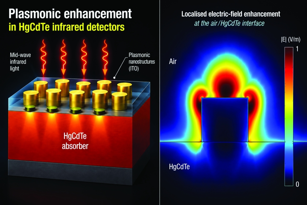
When infrared radiation interacts with our nanostructures, this generates collective oscillations of free electrons, known as surface plasmons. These resonances introduce highly localised electromagnetic fields in the vicinity of the nanostructures. In turn, there’s an increase in the optical energy density inside the HgCdTe absorber, boosting photon absorption within thinner layers. According to numerical modelling by our team, optimised plasmonic structures enhance midwave infrared absorption by approximately 15-18 percent, with higher gains achievable for specific geometries. Crucially, this enhancement comes without increasing absorber thickness or modifying the semiconductor material.
We employ what’s referred to as an effective-medium approach to model the optical response of nanostructured HgCdTe systems. Although structures involve nanoscale features, so quantum effects influence carrier behaviour, one can treat the interaction with infrared radiation with classical electromagnetic theory.
The structures we have considered include periodic nanostructure arrays, consisting of materials such as indium tin oxide embedded in air – it’s a combination that forms an effective optical layer, with a refractive index depending on geometry, spacing, and scattering characteristics. The effective index, which is strongly dependent on feature size, periodicity, and geometry, governs the resulting electric-field distribution, quantum efficiency, and absorption behaviour.
To ensure plasmonic enhancement, nanostructured material must exhibit a negative real permittivity at the detector’s operating wavelength. In the mid-wave infrared, there are a number of transparent conducting oxides satisfying this condition, behaving as metallic media while maintaining a comparatively low optical loss. When this happens, localised surface plasmons are excited at the interface with HgCdTe, producing intense near-field confinement and a strong coupling of optical energy into the absorber. This allows transparent conducting oxides to serve as effective plasmonic materials in spectral domains where conventional noble metals are less suitable.
The negative permittivity, needed to ensure a plasmonic resonance, governs how electromagnetic waves are confined and guided at the nanostructure interface. A negative permittivity ensures that the material supports surface-bound modes – they remain tightly confined near the interface rather than propagating into free space. Thanks to this confinement, there’s a significant increase in the local density of optical states, allowing more-efficient coupling of incident radiation into the absorber region.
From a device perspective, this behaviour is ideal, as it enhances the probability that photons contribute to carrier generation, and it reduces the likelihood that they are reflected or transmitted. The upshot is more efficient optical-to-electrical conversion, even in thin absorbers. It’s an improvement that’s particularly important in HgCdTe systems, where absorption, noise figures, and detector sensitivity are strongly linked to absorber thickness.
During our development of HgCdTe detectors that are enhanced with plasmonics, we uncovered small deviations between our measured and simulated values for absorption near the band edge, arising primarily from temperature sensitivity and detector operating conditions. Note that HgCdTe devices are typically optimised for low-temperature operation, and measurements performed under ambient conditions introduce fluctuations in detector response. This is particularly significant near the absorption edge, where small temperature variations may lead to noticeable differences in measured absorbance.
Why geometry matters
Details associated with geometry play a crucial role in determining how effectively plasmonic structures enhance absorption. We have shown that while the choice of material sets the fundamental electromagnetic response, the spatial distribution and intensity of the near field are governed by the shape and periodic arrangement of the nanostructures.

Figure 1. HgCdTe detector structures benefit from plasmonic nanostructures. This illustration highlights key geometric parameters and optical excitation.
Through systematic modelling we have uncovered some clear trends. Adopting symmetric structures, such as rings and cylinders, produces a relatively uniform field enhancement and reduced polarisation sensitivity, traits that are valued when constructing a detector. If highly asymmetric shapes are deployed, this can generate stronger localised fields – but potentially at the expense of an increased sensitivity to fabrication tolerances and illumination conditions.
The benefits of the plasmonic structure are significant, due to enhanced fields extending several micrometres into the HgCdTe absorber – that’s comparable to the thickness of conventional mid-wave absorbing layers. Thanks to this extension, there’s enhanced absorption, removing the need to resort to thicker material stacks.
Optimised structures
Our efforts to optimise plasmonic structures have been systematic, considering shapes that include rings, cylinders, and pyramids. This extensive investigation has revealed that the shape, size, and periodicity of the nanostructure have a decisive influence on absorption efficiency.
By tuning these parameters, we engineer absorption enhancement across the midwave infrared while retaining established semiconductor fabrication processes. We have found that transparent conducting oxides, such as indium tin oxide, are particularly attractive in this context. They offer metal-like optical behaviour with comparatively low loss in the infrared.
Our work has also highlighted practical trade offs. We have found that designs for maximising peak enhancement at a single wavelength may not perform as well across the broader spectral range required for imaging applications. This finding shows that what’s needed is to identify geometries that balance absorption gain with robustness and manufacturability.

Figure 2. Simulated electric-field distributions at the air/HgCdTe interface for different plasmonic nanostructure geometries: (A) reference structure without nanostructures, (B) spheres, (C) cylinder, (D) cones, and (E) rings. The simulations illustrate how nanostructure geometry influences localised field confinement and optical absorption behaviour. Insets show the optimisation parameters corresponding to each geometry.

Figure 3. Measured and simulated optical absorbance of HgCdTe in the mid-wave infrared spectral region for varying nanostructure widths, demonstrating enhanced absorption compared with conventional structures without plasmonic enhancement.
For our modelling, we use periodic boundary conditions to represent extended nanostructure arrays, allowing a single unit cell to capture the collective optical behaviour of large-area patterned surfaces (see Figure 1 and Figure 2).
The impact of these design choices on measured and simulated absorbance is evident (see Figure 3)
Practical considerations
If plasmonenhanced HgCdTe detectors are to be produced in volume, in addition to a strong optical performance, they must be manufacturable and reliable. Fortunately, these conditions should not be that demanding, as plasmonic elements can be implemented as surface features. This allows the introduction of electromagnetic field engineering without having to alter the underlying semiconductor growth process.
From a manufacturing standpoint, periodic nanostructures are particularly attractive, because they are compatible with standard lithographic techniques, and they tolerate realistic dimensional variations. But care is needed – we have identified that plasmonic enhancement introduces design trade-offs that must be managed. As mentioned before, while high absorption at targeted wavelengths is possible with strongly localised resonances, if the spectral response is overly narrow, this might not suit broadband imaging applications.
Another challenge is to control optical loss, so that there’s no excessive heating or impaired efficiency. Helping to fulfil this objective are transparent conducting oxides, which provide negative permittivity with a comparatively low loss in the infrared, and enable robust field confinement while preserving overall detector performance. By balancing these factors, plasmonic field engineering delivers meaningful gains, and builds on simulations to construct large-area, practical infrared detector systems.
The overall improvement in absorbance achieved through geometric optimisation is illustrated (see Figure 4).
Broader adoption
What began as an effort to enhance light-matter interaction in HgCdTe detectors has evolved into a broader design philosophy that’s been adopted and extended by other research groups across infrared photonics and optoelectronics. Our technology for enhancing optical absorption by engineering the electromagnetic environment has been shown to be robust and transferable across different materials, device architectures, and operating regimes.
Drawing on our efforts, researchers at the Army Research Laboratory have used gold-based plasmonic nanostructures to enhance infrared absorption in HgCdTe detectors. Although they employed noble metals, rather than transparent conducting oxides, they are also using localised surface resonances to increase the electric-field intensity at the detector interface and strengthen absorption in thin HgCdTe layers. Their success shows that our field-enhancement framework is not restricted to a specific material system, and can be implemented with different plasmonic platforms, depending on design constraints and fabrication considerations.
Extending these concepts beyond plasmonic materials, Mohammad Ariful Hoque Sojib and co-workers from Virginia Commonwealth University have shown that dielectric-grating-based architectures enhance the absorption in sub-wavelength HgCdTe layers by increasing the lateral optical propagation within the absorber. Although these designs do not rely on metallic plasmonics, they apply the same underlying mechanism of nanostructure-mediated light confinement we introduced to compensate for reduced absorber thickness.

Figure 4. Optimised plasmonic nanostructure arrays showing enhanced optical absorbance across the mid-wave infrared spectral range after geometric optimisation of the nanostructure parameters.

More advanced plasmonic implementations by Marco Vallone and co-workers from the Polytechnic University of Turin have involved investigating plasmonic cavity architectures for high-operating-temperature HgCdTe infrared detectors. Efforts by these researchers show that engineered resonances can improve absorption efficiency and detector performance at elevated temperatures.
Beyond device-level implementations, there’s work by researchers at Regensburg University, the Ioffe Institute, Poland’s Institute for High-Pressure Physics, and the Rzhanov Institute of Semiconductor Physics. Together, they examined symmetry-dependent transitions and photogalvanic effects in HgCdTe. This effort – relying on the underlying understanding of light–matter interaction and electromagnetic field distribution that underpins our modelling approach – shows that the impact of our original framework extends beyond device design into broader optoelectronic physics.
Taken together, these developments show that the research community is increasingly adopting electromagnetic field engineering as a primary strategy for improving infrared detector performance. The foundation for these investigations is the concepts introduced in our work.
Towards HOT detectors
Where the plasmonic enhancement may have the biggest impact is in high-operating-temperature (HOT) infrared detectors. At the system level, even modest improvements in absorption, resulting from the introduction of plasmonic nanostructures, may diminish cooling requirements, trim power consumption, and simplify architectures. For aerospace and defence platforms, where size, weight and energy budgets are tightly constrained, these gains could deliver an impact that’s well beyond the improvement in the detector itself. For example, the thinner absorber architectures that have a reduced cooling demand also offer a superior detector uniformity and an improved long-term stability. In addition, thanks to a reduced material volume, there can be a reduction in thermally activated noise sources and mitigation of mechanical stress introduced during repeated temperature cycling. For large infrared focal-plane arrays, these gains contribute to improved pixel-to-pixel consistency and reduced calibration overhead.
From a systems engineering perspective, if absorbers maintain a strong performance while operating closer to ambient temperature, this simplifies packaging requirements and broadens deployment options. Thanks to these advantages, detectors can be integrated into platforms where space, weight, and power constraints previously limited infrared capability.
Future directions
One promising direction that builds on our work is to integrate plasmonic nanostructures with advanced detector architectures, including multi-layer designs and hybrid photonic systems. There’s also the possibility of combining nanophotonics with computational optimisation techniques, and exploring increasingly large design spaces more efficiently.
Our plans include examining the behaviour of plasmon-enhanced HgCdTe structures under low-temperature operation, where changes in free-carrier concentration strengthen local field confinement and boost absorption efficiency. In parallel, we intend to investigate alternative transparent conducting oxides with higher carrier densities, such as fluorine-doped cadmium oxide and copper-doped aluminium oxide. These oxides should extend plasmonic enhancement across a broader range of operating conditions.
There’s also the possibility of turning to machine-learning-assisted design frameworks, which may accelerate identification of optimal nanostructure configurations and enable faster development cycles and improved detector performance. Taken together, these advances could position plasmonic HgCdTe detectors as a promising platform for next-generation infrared sensing technologies.
Ultimately, the engineering of infrared detectors will evolve, due to the convergence of plasmonics, advanced materials, and electromagnetic design.



