
UV lasers: MBE trumps MOCVD
Researchers from the University of Michigan are claiming to have broken new ground in epitaxy by producing the first edge-emitting lasers operating within the UV-B or UV-C by MBE.
The team’s lasers, which slash the threshold current for edge-emitters in this spectral range by more than an order of magnitude, will aid the development of on-chip UV sources for sensing, and could support metrology, water/air purification, disinfection, and quantum and defence-related photonic systems.
The success of the team may surprise many, given that MOCVD is seen as the superior growth technology for producing UVC laser diodes.
Commenting on this, group leader Zetian Mi remarks: “It has been generally believed that MBE, given its relatively low growth temperature, often leads to more defects and therefore limited performance for optoelectronic devices. However, this has changed over the last years, especially with the development of ultra-high-temperature molecular beam epitaxy by our group.”
Mi and his co-workers initially used their high-temperature MBE process to produce high-quality AlN and h-BN, before turning their attention to AlGaN-based heterostructures for UV lasers.
According to Mi, one of the strengths of MBE for the growth of mid- and deep-UV optoelectronic devices, and in particular laser diodes, is that it proceeds under an ultrahigh high vacuum that can significantly reduce the incorporation of impurities, such as oxygen and carbon – this is a significant concern for high-aluminium-content heterostructures.
In addition, compared to MOCVD, the growth chamber is relatively free of hydrogen, enabling more efficient p-type dopant activation; and thanks to precise monolayer control, MBE can realise atomically sharp heterointerfaces, which reduce charge-carrier trapping and enable more-efficient radiative recombination.
Fabrication of the team’s devices involved loading chemically cleaned Al-polar single-crystal AlN substrates into an MBE chamber. After thermal treatment of this material at 1000 °C, growth of the AlGaN heterostructure followed under metal-rich conditions.
Mi explains that using slightly metal-rich conditions promotes a gallium-adlayer during the growth of AlGaN. “Gallium, having a lower sticking coefficient than aluminium, promotes adatom mobility, thereby resulting in a smoother surface of the epilayers. This adlayer can also be readily removed when necessary, owing to the comparatively higher desorption rate of gallium.”
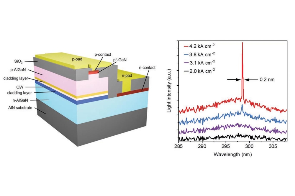
The team’s lasers feature a 3 nm-thick Al0.35Ga0.65N quantum well. It is sandwiched between a pair of 50 nm-thick undoped Al0.45Ga0.55N guide layers, which are bounded by cladding layers. The n-type cladding is 300 nm-thick silicon-doped Al0.35Ga0.65N, and the p-type cladding is a 250 nm-thick magnesium doped layer, compositionally graded from Al0.45Ga0.65N to Al0.85Ga0.15N.
Mi and co-workers used standard photolithography, dry and wet etching, and contact metallisation to produce ridge-waveguide lasers with a p-electrode width of 2 mm and a length of 600 mm.
Characterisation of the team’s lasers, using 1 ms pulses and a duty cycle of 1 percent, determined a peak emission wavelength of 298.5 nm, and a threshold current density of 3.4 kA cm-2. It is argued that this value – far less than that of 40-70 kA cm-2, which is reported for other electrically pumped UV-B laser diodes – can be reduced by supressing non-radiative recombination, cutting internal loss, improving current confinement, and incorporating advanced cavity-engineering strategies, such as optimised distributed Bragg reflectors and index-guided ridge geometries.
Mi says that the plans for the team are to investigate the design, epitaxy, fabrication, and characterisation of AlGaN-based UV-C laser diodes, pushing the operating wavelengths down to 265 nm. “Moreover, we are working to achieve high-output-power mid- and deep- UV laser diodes for more practical applications.”
Reference
H. Yu et al. Appl. Phys. Lett 128 143501 (2026)


