
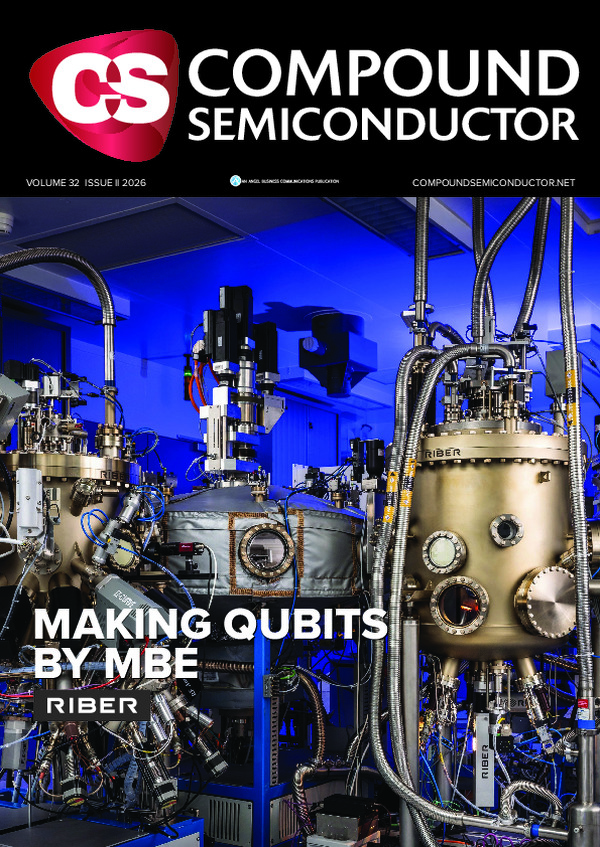
Making qubits by MBE
MBE excels in the growth of structures for quantum computing that combine layers of semiconductors and superconductors.
BY CLAUDINE PAYEN, YOURI ROUSSEAU, ROMAIN RICHARD FROM RIBER AND ALEXANDRE ARNOULT, SÉBASTIEN PLISSARD, QUENTIN GRAVELIER AND HUGUES GRANIER FROM LAAS-CNRS
The first quantum revolution, associated with the birth of quantum theory, took place at the start of the twentieth century. Humanity is now building on this as we enter the second quantum revolution, which is characterised by the manipulation, control and exploitation of quantum phenomena, with the objective of creating new technological objects. A key part of this era is the introduction of quantum computing.
This particular breakthrough is so exciting that it’s not just being reported in the technical press – stories of quantum computing are also appearing in mainstream media. An ever-growing number of laboratories are driving progress, along with the major research centres of the five big tech companies, collectively referred to as GAFAM: Google (Alphabet), Amazon, Meta (formerly Facebook), Apple, and Microsoft. Efforts by these institutions are directed at providing innovative, high-performance solutions in areas such as simulation, particularly in chemistry and pharmacology, as well as encrypted data exchange, and flux movement optimisation – the latter relates to the likes of car traffic and logistics.

Transmission electron microscopy image, showing
the perfect interface of 20 nm-thick aluminium (111) grown on a GaAs
(001) substrate. Results from Epicentre.
The goal of a quantum computer is not limited to using quantum physics for its operation. The aim is to also ensure that computations are quantum, that is, the way calculations are performed is also quantum related. To accomplish this, computation must involve two key quantum properties: the superposition of states and quantum entanglement.
Engineers that are working towards this have several options for building a quantum computer. To transport information, they can employ trapped ions, photons, electron spins, nitrogen-doped diamond cavities, Josephson-effect superconductors, or Majorana fermions (fermions that are their own antiparticles, and appear in certain materials, including hybrid systems of superconductors (Al, Nb…) and topological insulators (BiSe, BiTe..)). All these particles are known as quantum bits or, for short, qubits. Only time will tell which of these approaches prove successful, and as of today nothing has been definitively established.
Among the different ways to create a qubit, three may benefit from MBE: Majorama fermions, Josephson junction superconductors and photons.
The key strengths of MBE are its ultra-clean ultra-high vacuum environment, the use of high-purity material that enables the growth of perfectly defect-free interfaces, and exceptional control that ensures monolayer precision and crystalline perfection.
To support the development of quantum computing, our company, Riber, which has been making MBE systems for more than 45 years, has recently launched a new platform with the capability to produce semiconductor-superconductor structures within a single ultra-high vacuum environment.

First Josephson junction achieved in the framework of Epicentre by Sébastien Plissard and his team.
The Supra hybrid platform
Our hybrid platform called Supra – derived from the French word for superconductor, ‘supraconducteur’, is a fully automated ultra-high vacuum system that’s dedicated to the growth of semiconductor–superconductor heterostructures. Developed in close collaboration with LAAS-CNRS Toulouse within the joint laboratory Epicentre, it provides unprecedented control over epitaxial interfaces, opening new pathways for producing higher-performance qubits.
When developing our Supra hybrid platform, we have drawn on our long-standing expertise in the MBE of III–V semiconductors. Within this new platform is a primary III-V growth chamber that’s optimised for the fabrication of high-purity heterostructures of compound semiconductors.
This chamber is directly connected, under ultra-high vacuum, to a new, patented cryogenic metal growth reactor that’s dedicated to superconducting materials. In this chamber engineers can deposit thin superconducting films, such as aluminium, tin, lead and specific alloys, directly onto semiconductor surfaces at temperatures below 100 K. Thanks to full-wafer in-situ deposition on rotating substrates, our platform provides excellent thickness uniformity on wafers with diameters up to 100 mm, while in-vacuum transfer guarantees oxide-free, contamination-free interfaces.
Critical cryogenic growth
For superconductors, shifting from conventional deposition temperatures to the cryogenic realm delivers decisive advantages. Cryogenic temperatures suppress the surface diffusion of metal adatoms, leading to smooth, continuous films with reduced grain boundaries and structural disorder. What’s more, this growth regime minimises thickness inhomogeneities to yield ultra-flat superconducting layers with low dissipation. Equally important, deposition at cryogenic temperatures strongly suppresses interdiffusion and chemical reactions at semiconductor-superconductor interfaces. By preventing alloy formation and interface roughening, our system preserves atomically abrupt, chemically intact interfaces. This exceptional interface quality ensures high transparency and strong superconducting proximity effects – they are key requirements for high-performance Josephson junctions and hybrid quantum devices.
For aluminium in particular, a low growth temperature enables the stabilisation of specific crystalline orientations and epitaxial relationships, requirements that are difficult to obtain at higher temperatures. Structurally coherent films are crucial, translating directly into improved device uniformity, narrower distributions of critical current, and reduced leakage in Josephson junctions. All three are essential for scalable quantum circuits.
Benefits of cryogenic growth are also seen when viewed from a quantum device perspective. There’s reduced structural disorder and pristine interfaces, two valued characteristics that lead to a lower quasiparticle density, reduced noise sources, and improved coherence times – central metrics for qubit performance.

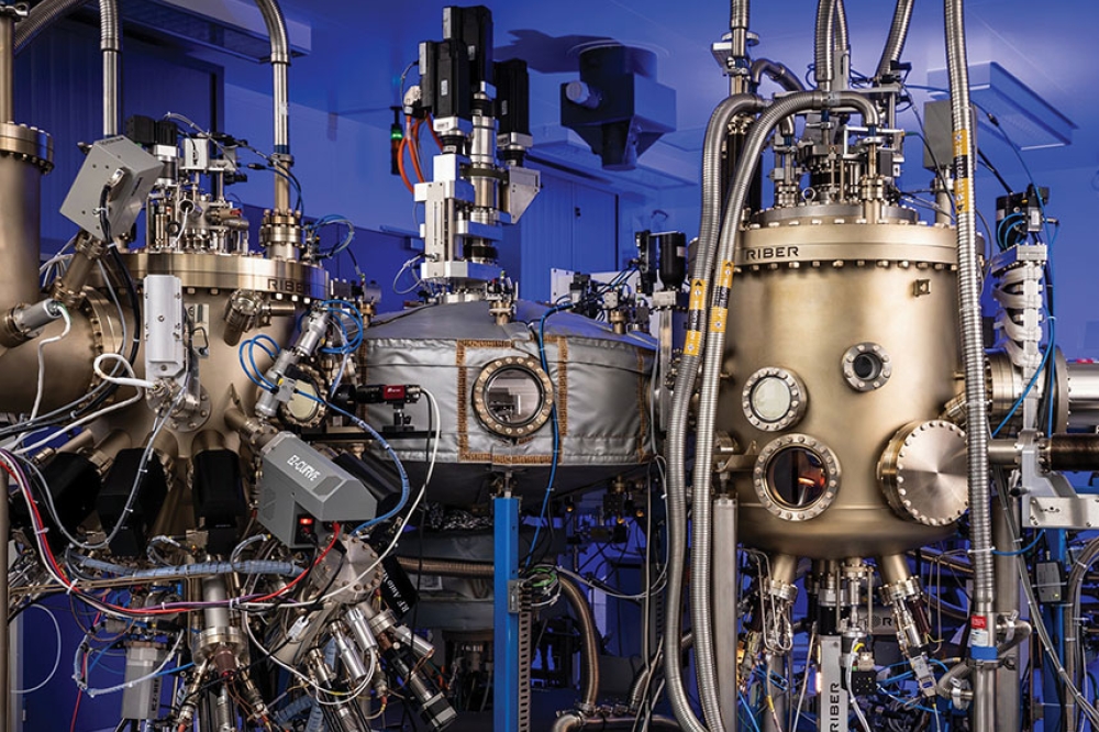
Supra Platform at Epicentre, a joint laboratory between Riber and LAAS-CNRS member of Renatech network.
Our platform also provides dedicated oxidation capabilities, either within the cryogenic chamber or in a specific oxidation module. This allows precise, reproducible formation of ultra-thin tunnel barriers under controlled conditions.
By maintaining the entire semiconductor-superconductor growth and oxidation sequence under ultra-high vacuum, we eliminate uncontrolled oxidation and contamination that’s typically associated with ex-situ processing.
One of the weaknesses of traditional fabrication methods is that they often expose the superconducting film to air during processing, leading to uncontrolled oxidation and interface contamination. By contrast, our hybrid platform maintains the entire semiconductor-superconductor growth sequence under ultra-high vacuum, to ensure epitaxial interfaces with superior transparency and stability.
We have evaluated the capabilities of our Supra hybrid platform by growing and characterising a structure on a GaAs (001) substrate that consists of a thin epitaxial aluminium (111) layer, a thin Al₂O₃ tunnel barrier, and a polycrystalline aluminium top electrode. For the growth of the aluminium layer, deposition took place at 90 K, a low temperature that strongly reduced the surface mobility of aluminium adatoms, supressed long-range diffusion, and limited the formation of misoriented nuclei. Due to this, aluminium grows epitaxially on GaAs (001) with a well-defined (111) orientation.
Inspecting this structure using cross-sectional electron microscopy provides images with uniform contrast and an absence of visible grain boundaries. This form of microscopy also confirms the single-crystalline nature of the aluminium (111) layer.
During the growth of this superconductor-semiconductor stack, the thin Al₂O₃ layer is formed by controlled oxidation of the epitaxial aluminium surface. There is a lack of long-range order in the oxide, indicating an amorphous structure. This leads to an aluminium (111) epitaxial/Al₂O₃ amorphous/aluminium polycrystalline stack that combines a high-quality superconducting base electrode with a robust tunnel barrier. It’s a combination that’s well-suited to Josephson junctions integrated on semiconductor platforms. This technology is a candidate for superconducting electronics and quantum devices.
Beyond semiconductor-superconductor fabrication, our platform is a contender for producing Josephson junctions, thanks to a chamber that can grow superconducting material at a low temperature. It should be noted that the Supra chamber allows growth with wafer rotation, to ensure high uniformity across the whole wafer.

Aluminium deposition on a GaAs substrate with 2D morphology and monocrystalline phase. X-ray diffraction measurement of a 18 nm-thick aluminium film grown at 92K on a GaAs (001) substrate. Epicentre was able to maintain substrate temperature below 100K during aluminium growth for more than 3 hours.
Towards early industrialisation
With a combination of ultra-high vacuum integrity, full automation, recipe-based process control, and real-time in-situ monitoring instruments that are based on optical measurements and, our Supra platform provides a level of reproducibility suited not only to academic research but also the early-stage industrialisation of quantum technologies. As this emerging field moves toward scalable architectures, the ability to fabricate uniform hybrid interfaces and Josephson junctions across full wafers will become indispensable.
By integrating III-V semiconductor growth, cryogenic superconductor deposition and controlled oxidation in a single ultra-high vacuum environment, our hybrid platform minimises contamination, increases uniformity and simplifies workflow – they are three key requirements when transitioning from laboratory-scale demonstrations to manufacturable quantum devices.
Supporting our development of quantum-related technologies is the Epicentre, a joint laboratory between Riber and the CNRS Laboratory for Analysis and Architecture of Systems (LAAS-CNRS) in Toulouse – it’s one of the largest in-house units of the French National Centre for Scientific Research (CNRS). Working together, we have already used the Supra chamber to demonstrate high-quality aluminium growth on GaAs substrates, with monocrystalline aluminium films grown below 100 K for several hours, atomically sharp interfaces confirmed by transmission electron microscopy, and the realisation of the first Josephson junctions, developed by Sébastien Plissard and his team at LAAS-CNRS.
Beyond device validation, the Epicentre is playing a central role in addressing key technological barriers that have previously limited the integration of cryogenic superconductor growth within an MBE environment. One major challenge that we have tackled through the development of the Supra chamber is the design of a cryogenic metal growth chamber that’s compatible with ultra-high vacuum and full-wafer MBE standards, while maintaining precise thermal stability below 100 K over extended deposition times. To realise such stability, we had to develop a dedicated cryogenic architecture that ensures uniform cooling, controlled thermal gradients, and mechanical stability compatible with wafer rotation.
Another critical hurdle that we’ve overcome is the preservation of interface purity during cryogenic deposition. At low temperature, conventional effusion and shutter designs could induce parasitic condensation, flux instabilities, and uncontrolled background deposition. Our Supra chamber architecture overcomes these limitations through a patented source-to-substrate geometry and thermal management scheme, enabling a stable metal flux, reproducible growth rates, and the suppression of unwanted condensation on cold surfaces.
An equally important challenge is enabling in-situ, contamination-free transfer between semiconductor growth, cryogenic metal deposition, and controlled oxidation. Our Supra hybrid platform, which integrates an ultra-high-vacuum-connected cluster design, ensures that the semiconductor–superconductor interface is never exposed to ambient conditions. This capability is essential for maintaining chemically abrupt interfaces and forming reproducible tunnel barriers.
We will continue to advance the capabilities of our hybrid platform and share our results.
Efforts related to the latter including a presentation by Sébastien Plissard at the International Workshop on Superconductor-Semiconductor Hybrids 2026 that will highlight Supra’s role as a key enabling platform in next-generation hybrid quantum technologies.


