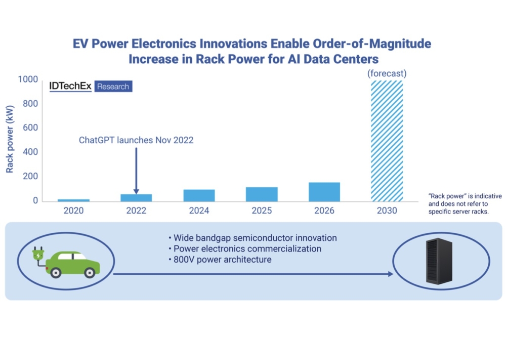
Retrospective - 1995-2004
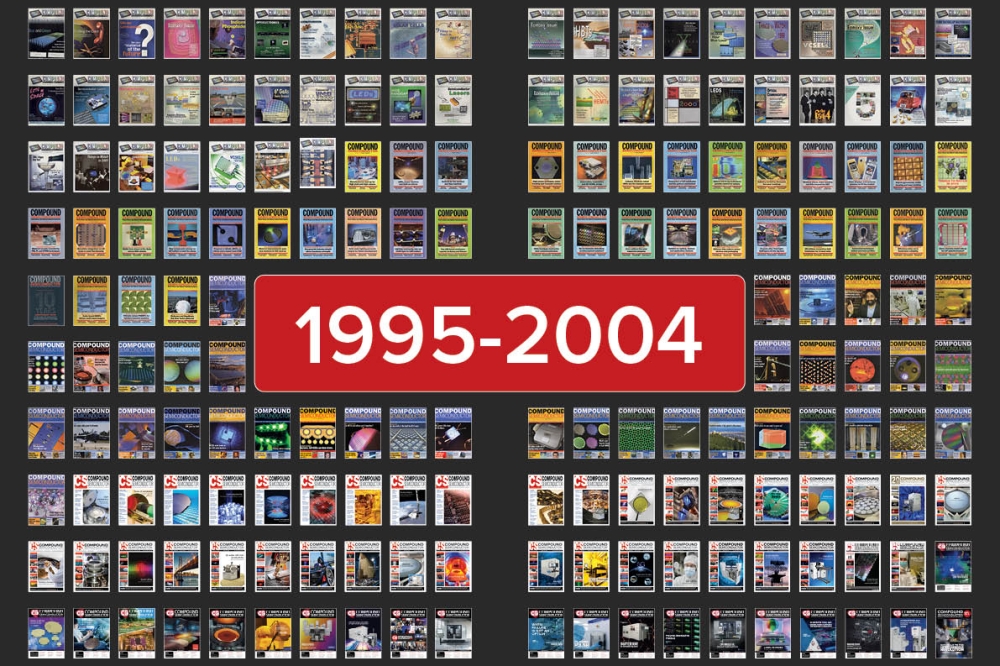
We look back at some of the biggest stories from the first ten years of Compound Semiconductor magazine, including invention of the GaN laser, the rise and fall of digital GaAs, and the birth of commercial SiC power devices.
A brilliant laser
1995. By summer 1995, Shuji Nakamura, trailblazer of efficient blue LEDs, had already become an industry celebrity. After inventing this device in 1993, he remained in the limelight by setting a series of ever higher benchmarks for the performance of this light-emitting chip. These successes enriched his standing within the tech pantheon of all-time greats and brought many accolades, including the biggest of all, a Nobel Prize for Physics, coming in 2014. But he got even greater pleasure from seeing his work laying a foundation for a lighting revolution.
While Nakamura is undoubtedly renowned for contributions to the development of the GaN LED, it is by no means the only ubiquitous device he has invented. He is also the originator of the cousin of the GaN LED, the GaN laser diode. The latter is an astonishing triumph. While many manufacturers are making millions of GaN LEDs every month, 30 years on from its introduction, there are still only two high-volume makers of the GaN laser diode: Nichia, where Nakamura worked throughout the 1990s; and Osram Opto Semiconductors of Regensburg, Germany.
Nakamura’s laser breakthrough came in late 1995, with news breaking on 12 December. Nichia’s greatest engineer appeared on TV later that month on a national evening news broadcast, demonstrating his wonderful new device.
By early 1996, details of the laser diode started to appear in the scientific press. A paper in the Japanese Journal of Applied Physics described a 30 µm-wide, 1500 µm-long stripe laser grown on a sapphire substrate. Emitting at 417 nm, it had an active region containing 26 quantum wells, each made from a 2.5 nm-thick layer of In0.2Ga0.8N. To get this device to lase, the voltage had to be cranked up to 34 V. Driven in pulsed mode at even higher voltages, this chip produced an output of more than 200 mW. Encouragingly, this laser showed no signs of degradation after two hours of operation.
Even before its debut, the entire optoelectronic industry had little doubt regarding the killer application for this short-wavelength laser diode. Back then most music lovers bought CDs, VHS recorders were on the verge of being replaced by DVD players, and even better picture quality was now on the horizon, thanks to a five-fold hike in storage density enabled by blue-violet lasers.
Those keen to splash out on a new generation of disc players that would allow them to watch high-definition movies in their own homes had a really tough time. Early adopters began by getting caught up in a format war between the advocates of HD DVD technology and those giving their backing to Blu-ray. When that had been resolved, allowing customers to pay top whack for one of the first Blu-ray players that hit the shelves in Japan in 2003, further frustration followed – those early adopters had to wait several years for the launch of the first titles.
Fortunately, some good years followed, providing a growing, lucrative market for the blue laser diode. Since then the uptake of streaming services has sent sales of Blu-ray players into terminal decline – but as this door has shut, several others have opened. Blue lasers are now being deployed alongside red and green variants in colour projectors, and used in copper welding systems, where they operate at an absorption sweet spot, enabling excellent welds. There is also the possibility that one day lasers will replace LEDs in general lighting – so maybe, just maybe, there will come a time when society is as thankful to Nakamura for his laser as they are for his LED.

Shuji Nakamura, inventor of efficient GaN LEDs and GaN lasers, sitting next to Nobuo Ogawa, founder of Nichia. Credit: Bob Johnstone.
Photovoltaics fly high
1996. Back in 1985, very few owned a mobile phone. Those that did included Karen Bertinger, the wife of a Motorola executive, who tried to reach her husband while holidaying in the Caribbean. The call failed to get through, convincing intended recipient Barry Bertinger of the need for a truly global wireless communication network. To build this, Motorola founded and financed Iridium, a spin out that would advance telephony through the launch of 66 satellites, all placed in low-earth orbits.
By 1996, makers of III-V photovoltaics were busy producing devices for powering these satellites. Although silicon cells were still winning sales in the space sector, single-junction GaAs devices were in the ascendency. Despite costing five-to-eight times as much as their silicon siblings, they were favoured, due to their higher efficiency. At the start of their life, they had an efficiency 25 percent higher – and crucially, at the end of life, after being battered by radiation, they were 40 percent to 60 percent more efficient. Given that each Iridium satellite required 24 m2 of GaAs cells, using these devices rather than those made from silicon led to a significant reduction in the solar cell footprint.
Helping to fulfil orders for GaAs solar cells were a pair of Californian photovoltaic manufacturers: Spectrolab, at the time a subsidiary of Hughes and now part of Boeing; and Tecstar. For the latter, thanks to involvement in the Iridium project, in 1996 production totalled 200,000 3-inch wafers, equating to 140 kW of power.
Engineers produced these cells on germanium substrates. They were half the price of those made from GaAs, and much stronger. Use of germanium substrates generated much business for the makers of the raw material – the price of high-purity polycrystalline germanium rocketed, climbing by a factor of seven in just 18 months – and ramped sales for two leading substrate makers, US firm Eagle Pitcher and the Belgium outfit Union Minière, now known as Umicore. In 1996 germanium substrate consumption totalled between 300,000 and 500,000, with sizes ranging from 1.5 inch to 4 inch.
On 1 November, 1998, the Iridium network launched to much fanfare, with the first call placed between US Vice President Al Gore and Gilbert Grosvenor, great-grandson of Alexander Graham Bell. However, despite this great publicity, the service never caught on. Potential customers balked at paying $2500 for the handset. Dropping this to $1495 and slashing service costs failed to generate enough business, and even by the end of 1999, Iridium had just 15,000 subscribers, a far cry from an anticipated 500,000. An inevitable filing for bankruptcy followed.
Failure of the venture took its toll on photovoltaic maker Tecstar. In 2001, it tried to branch out into LED epiwafers. Diversification did not go well, and in 2002 Tecstar’s management decided to call it a day, selling it solar division to Emcore for $21 million. Today, the technology is in the hands of Rocket Lab. In 2022 Rocket Lab bought SolAero, which formed in late 2014 through the sale of Emcore’s solar power business.

With 66 satellites each requiring 24 m2 of GaAs solar cells, the Iridium project, which aimed to provide global cellular coverage, generated much revenue for the III-V photovoltaics industry. Credit: Eric Long, National Air and Space Museum, Smithsonian Institution.
Growth for gallium arsenide
1997. Owning a mobile may not have been the norm in the early 1990s, but it became increasingly common towards the turn of the millennium. The uptake of these handsets helped to swell the sales of makers of GaAs microelectronics, and provided the impetus for several of these firms to reach milestones, including three in 1997: the launch of RFMD on the stock market, the shipment of Rockwell’s two-millionth HBT, and Anadigics’ sale of its millionth GaAs IC.
RFMD, now part of Qorvo, started out as a fabless supplier of GaAs MESFETs, silicon bipolar devices, and HBTs, which provided 85 percent of sales. As demand for the latter ramped, RFMD couldn’t keep pace, losing a key contract with Qualcomm.
To prevent this from happening again, RFMD built its 4-inch GaAs fab in Greesnsboro, NC, in the late 1990s. Constructed in two phases, the facility initially produced 10,000 wafers per year, before eventually increasing to 25,000. Funding for this facility came from an IPO, supported by RFMD’s source of HBT wafers, TRW. It would become RFMD’s biggest shareholder, taking a 31.1 percent stake in the company.
For Rockwell Semiconductor Systems, the latter half of the 1990s will be remembered for an explosive ramp in the production of its HBTs, made in its 4-inch fab. During the 18 months spanning the beginning of 1996 to the middle of 1997, production at this company – which went on to form Skyworks Solutions in 2002 through a merger with Alpha Industries – mushroomed from just 10,000 units per month to 70 times that figure. Buyers of these HBTs included Qualcomm and Samsung. Both valued this class of transistor for its combination of excellent linearity and high efficiency, attributes ideal for making handsets based on CDMA technology that featured long talk times.
Rockwell faced competition for this business from Anadigics, which had shipped more than a million GaAs ICs supporting the CDMA standard by summer 1997. While most of Rockwell’s HBTs were being incorporated into phones operating in the 800 MHz to 900 MHz band, parts for Anadigics were providing amplification in transmitters of handsets using spectrum at 1900 MHz.
These higher-frequency products, based on Anadigics core technology, the MESFET, initially positioned the company for future success – but further ahead, contributed to its decline.
By the late 1990s, handset makers had shifted from using 6 V batteries to those providing 4.5 V and then just 3 V. This played into the hands of the increasingly price-competitive HBT. By the early 2000s, Anadigics ceased production of its MESFET, fighting back by developing a new generation of HBT.
Instead of having an AlGaAs emitter, it used InGaP. This refinement increased the HBT’s reliability, bolstered its high-temperature operation and improved its linearity. Anadigics’ product eventually proved a hit with handset makers, giving the company a healthy share of the 3G market.
A fabulous fab
1998. When you think of high-volume manufacture of GaAs microelectronic devices, you’ll probably think of HBTs for smartphones. But that’s not the only market that has existed. In the telecommunications sector, a great deal of GaAs has been produced for laser and modulator drivers, multiplexers, demultiplexers, transimpedance amplifiers, clocks, and data-recovery circuits. In all these components, the higher speeds wrought by GaAs over silicon CMOS yielded higher bit rates.
Back in 1998, when GaAs devices for the telecoms sector were flying off the shelves, Vitesse increased its production capacity by building the world’s first 6-inch GaAs fab.
Unlike most construction projects, where deadlines come and go, Vitesse’s facility in Colorado Springs, CO, came in more than three months ahead of schedule. The first products, featuring GaAs MESFET technology, came off the line in early 1998, and in the third quarter of the year the company shipped $15 million of chips, based on 16 different products.
Vitesse, which also led the world in the migration from 3-inch to 4-inch GaAs production, built the 6-inch fab to cut the cost per die. Despite incurring a 25 percent hike in substrate-cost-per-unit-area, the switch to larger wafers delivered a 40 percent reduction at the die level.
In the markets that Vitesse served, its technology had to continue to advance so that it could maintain a healthy lead over products based on silicon CMOS.
The bursting of the dot.com bubble dealt a cruel blow, causing sales for Vitesse’s 40 Gbit/s devices to collapse and not recover before a 90 nm silicon process had caught up. This ultimately led to the closure of Vitesse’s GaAs fab in 2003.
After that, the company shifted focus, concentrating on silicon-based products for the metro, enterprise and storage market; and used its 4-inch InP fab to make high-speed electronic devices. The final chapter in the company’s history came in 2015, with its acquisition by Microsemi.
Even today, a 6-inch fab represents the state-of-the art for producing GaAs transistors. This might suggest that in the last two decades progress in chip manufacture has stalled. But consider this: in silicon CMOS fabs, the rapid advances in wafer sizes through the last three decades of the twentieth century have not continued into this millennium, and there may never be a 450 mm silicon fab.
For silicon, the 300 mm fab appears to be the sweet spot for production, with the investment required for any larger size failing to offer a suitable return – and for GaAs, could the same apply to the 6-inch line?
The perfect marriage
1999. What makes for an ideal merger? In a nutshell, it occurs when the result is greater than the sum of its parts.
That took place when Epitaxial Products International (EPI) joined forces with Quantum Epitaxial Design (QED) in 1999 to create IQE, the world’s largest epiwafer supplier. QED of Bethlehem, PA, had built up its business by supplying MBE-grown wafers, used to make electronic devices, to a predominantly domestic market; while UK-based EPI had focused on optoelectronic epiwafers, with two-thirds of its sales coming from Europe and Asia.
The merged entity, offering a dual source of supply for some products, promised to be a resounding global success, drawing on the growing businesses of both companies. Sales at QED were increasing at a compound annual growth rate of 40 percent, while at EPI they were ramping at 30 percent. To cater for greater demand both sites had capacity expansion plans in place. QED had an order in for an MBE reactor capable of producing multiple 6-inch wafers from a single run, and EPI, which had recently increased the size of its facility, had placed orders for multi-wafer MOCVD tools. Helping to fund these expansion plans, IQE raised $70 million in an IPO, launching on the EASDAQ, the European version of NASDAQ, in summer 1999.
Since then, IQE has strengthened its leading position in the epiwafer market. In 2006, it acquired the epi business of Emcore; the following year it bought MBE Technologies of Singapore; and in 2012 it acquired the epi business of RFMD. It has also broadened its portfolio. The purchase Galaxy Semiconductor of Spokane, WA, in 2010, equipped the company with capability in antimony substrates and infrared technology; in 2012, the investment in Solar Junction strengthened expertise in multi-junction solar cells; and in 2018, the acquisition of Translucent’s technology brought capability in crystalline rare-earth oxides on board, enabling compound semiconductor films to be grown on silicon wafers.
However, the last few years have been far from stellar for this colossus of epiwafer manufacturing. Sales are well down from their peak of £178 million in 2020 and after decades of leadership from the company’s charismatic founder, Drew Nelson, his replacement, Americo Lemos, has been sacked after less than three years in charge. Turning all this around will not be easy, but thanks to operation in diverse markets, a return to better days is far from impossible.
In the late 1990s and early 2000s GaAs fabs were transitioning to larger wafers. Injecting some humour into the race to gain bragging rights with ever larger lines, TriQuint provided ‘evidence’ of its 6-foot fab in a series of images, described in chronological order. (top left) TriQuint announced the start-up of the industry’s first 72-inch wafer assembly line by circulating a press release at the GaAs Mantech conference held in 1999. (top middle). TriQuint then revealed that some of its engineers had been working frantically to prevent heavy lifting. “Man these are some big GaAs-wafers,” commented one operator (top centre). In the next picture story (top right), a TriQuint technician remarked:
“I don’t know what happened, it just fell off the wand!” TriQuint went on to explain how equipment maintenance can prove to be quite a chore in a 72-inch wafer fab. This equipment engineer is inspecting just one of the many massive vacuum chambers used in the evaporation process. (bottom left) In the final release (bottom right), TriQuint reported how excitement built at the 72-inch wafer plant as the first finished wafers were distributed through the ‘Silicon Forest’.

In 1999 the merger of UK-based Epitaxial Products International and US-based Quantum Epitaxial Design spawned IQE, which launched on the European equivalent of the NASDAQ.
Giddy highs
2000. Internet traffic soared in the run up to the
millennium, placing tremendous strain on optical communication infrastructure.
Carriers addressed this by beefing up network capacity. This created an optical
component sector worth almost $10 billion and tipped to increase at a compound
annual growth rate of 40 percent. Makers of III-V optoelectronics were
well-positioned to benefit from this ramp, as their devices accounted for up to
half that market.
Understandably, frantic carriers did not want to deal with numerous component suppliers. They longed for one-stop shops, ideally offering modules that would drop into their networks.
To cater for this demand, acquisitions ran rife in the components sector. JDS Uniphase (JDSU), formed in June 1999 through the merger of the Canadian outfit JDS Optics and the US firm Uniphase, led this spending spree. In late 1999 JDSU signed a deal worth $400 million for photodetector maker Epitaxx, and in 2000 it made three monumental acquisitions: it snapped up Optical Coating Laboratory for $6.2 billion, E-Tek Dynamics for $15 billion and SDL Lasers for a whopping $41 billion.
Once the dot.com bubble had started to burst in the first few months of the new millennium, everyone knew the folly of buying a company for a figure that is many times more than its annual revenue. That made the purchase of SDL, for which JDSU had forked out a sum equating to 142 times the annual revenue, an outrageous blunder. Hindsight exposed any notion of a new world order, rampant in the giddy highs, and traditional economics were back with a vengeance.
During 2000, inventory corrections kicked in within the supply chain, driving down margins. On 30 June of that year JDSU had the dubious distinction of reporting the biggest ever annual corporate loss – an eye-watering $ 56.1 billion (taking inflation into account, it’s now in third place, behind AOL Time Warner and the American International Group). However, for JDSU this loss was predominantly on paper. The vast majority of the $56.1 billion came from a write down of goodwill associated with various acquisitions, which were primarily all-stock deals.
For investors, the downturn in company fortunes could not be dismissed so easily. In March 2000, spurred on by analyst claims that out-of-the-box visionaries were leading a great company in exactly the right place at the right time, shares in this Wall Street ‘darling’ peak at $1200. Go forward a few years and they had fallen by more than 99 percent.
The company’s leaders sold some of their shares near their peak, leading to accusations of fraud and insider trading. Some joked that JDSU now stood for Just Don’t Sue Us – but those representing the state of Connecticut did just that, hoping to recover losses from a pension fund. The case, filed in 2002, came to court five years on, with management cleared of fraud.
By then the company CEO of the glory days, Kevin Kalkhoven, had retired, using part of his wealth for philanthropic ventures. He also funded a car-racing team that notched up five victories, including the Indianapolis 500 in 2013.
As for JDSU, it no longer exists. The prolonged downturn in the optical component business took a heavy toll, with the company shedding 80 percent of its workforce and closing 29 sites. In August 2015 the company split, forming network test and measurement specialist, Viavi Solutions and the laser manufacturer Lumentum.

Kevin Kalkhoven, former JDSU CEO, co-founded PKV Racing, later known as KV Racing Technology. This team competed in both the Champ Car World Series and the IndyCar series, amassing five wins, including the 2013 Indianapolis 500.
A powerful start
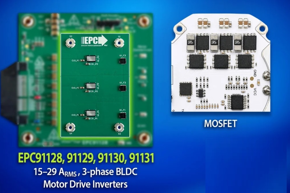
2001. What marked the beginning of the wide bandgap power
electronic industry? It is surely Infineon’s the launch of the SiC Schottky
barrier diode, the first wide bandgap power electronic product to hit the
market.
When this device made its debut in 2001, it filled a gap. Silicon and GaAs Schottky barrier diodes were limited to blocking below 250 V to avoid very high leakage currents, exacerbated at high temperatures. Infineon’s pair of variants could handle 300 V and 600 V while carrying up to 1 A, and were far better at handling heat, giving them an edge for deployment in power supplies.
Infineon, which made these devices from 2-inch SiC wafers at its fab in Villach, Austria, targeted power supplies operating between 200 W and 1000 W. Used in that manner, the company’s diodes featured in servers and wireless base stations. The designers that made the switch from silicon diodes to those made from SiC were well rewarded. Their supplies were more reliable and more efficient, and they could be smaller and lighter, as the SiC diodes allowed the operating frequency to increase, opening the door to a reduction in the size and weight of passive components.
Infineon’s first generation of SiC diodes sported a simple architecture, selected to try and minimise costs that were dominated by pricey 2-inch SiC substrates. Since then, substrates have increased in size and quality and fallen in price, and diodes have been through several iterations, increasing in complexity. By 2018, Infineon had reached its sixth generation of 650 V SiC Schottky barrier diodes, a family of devices capable of handling currents ranging from 4 A to 20 A. These are still available, alongside fifth-generation variants with blocking voltages of 1.2 kV and 2 kV, and current ratings of up to 80 A and 40 A, respectively.

The birth of the wide bandgap industry came in 2001, with Infineon’s launch of the SiC Schottky barrier diode.
Hooray for handsets
2002. The compound semiconductor industry can never be
accused of putting all its eggs in one basket. But at the start of this
century, it certainly placed two of its largest in there. Back then, handsets
provided the killer applications for the two biggest sellers: LEDs, used to
backlight screens, illuminate keypads, and provide camera flash; and GaAs
transistors, employed to amplify and switch RF signals.
When the mobile phone industry was in its infancy, the focus would have been on attracting new customers. But it would not have taken long before efforts broadened to include attempts to woo owners to upgrade their devices. In 2002, the cool new features were colour screens, built-in cameras, and picture and photo-messaging services. In Japan, mobile network operator J-phone offered those that purchased a new handset the opportunity to send video clips lasting 5 seconds.
Over the last two decades, the leading brands have changed markedly, shifting the fortunes of the makers of GaAs microelectronics. In early 2002, when phones supporting 2.5G led the way,
Nokia dominated the market with a share of more than 35 percent, with its handset production providing the GaAs HBT manufacturer RFMD with about half its shipments. Motorola occupied second spot with 16 percent of the market, followed by Samsung, Siemens, and Sony Ericsson.
Fast forward to 2024 and Apple had moved up to pole position with a 19 percent share, closely followed by Samsung. There has also been a substantial rise annual phones sales.
In 2002, handset sales totalled just over 400 million units, and since 2014 this figure has remained above the billion per annum, peaking in 2018 at just over 1.5 billion.

The introduction of colour screens in handsets in the early years of this millennium helped swell sales of LEDs.
Tumultuous times for telecos
2003. After economic shocks, such as those caused by the
pandemic or Russia’s invasion of Ukraine, financial recovery may take many
forms. We will hanker for a “V” – that is, after a sharp decline there will be
an equally sharp rise that speeds us to a time of steady, sustained growth. But
often the best we can realistically hope for is a “U”, with a few tough
quarters in store before a return to better days. What we are desperate to
avoid is an “L”, a decline that leaves a permanent scar on the economy.
Sometimes some sectors will experience an “L”, even when the
general economy is on the up. That happened to component makers within the
telecommunications market in the ‘noughties’, leading to a flurry of activity
in 2003. When the dot.com bubble started to burst, the III-V chipmakers
operating in this industry initially put the problem
down to inventory corrections.
However, by 2003, with orders still failing to pick up, it became clearer that the real issue was long-term over-capacity. This cannot be fixed when facilities change hands – all that can do is potentially increase production efficiency. The hard reality is that when there are more fabs than needed to supply demand, some have to be closed and workers laid off.
This chain of events can be seen in the activity at Bookham. Shortly after the bubble burst, it picked up Nortel Networks optical components division and Marconi’s optical components business. In 2003, to try and streamline operations, it started relocating Nortel’s former InP chipmaking facility in Ottawa, Canada, to the ex-Marconi facility in Caswell, UK. In addition, it moved the semi-automated line for laser assembly and test from its site in Zurich, Switzerland, to its facility in Paignton, UK. At that site, used to assemble optical chips into packaged products, headcount had already plummeted from a heyday figure of 7000 to just 800.
When a sector is struggling and showing no signs of recovery, it’s a good idea to diversify into new markets. In late 2003 Bookham positioned itself to do just that, purchasing Ignis Optics, a maker of transceivers for datacom networks, and New Focus, a provider of photonics and microwave products for semiconductor, biotech, defence and research industries.
In 2003 another major shift in the optical components landscape came from Avanex’s acquisitions of divisions of Alcatel and Corning. The former calved off Alcatel Optronics, while the later parted company with its optical components’ plants in Milan, Italy, and its optical amplifier facility in Erwin, NY. Corning’s restructuring also involved the closure of its Lasertron pump laser facility, purchased in a $1.8 billion stock deal in November 1999.
Further changes within the components sector in 2003 included: ASIP, a maker of InP optoelectronic components, purchasing struggling rival ThreeFive Photonics; integration of the optical chip processing lines at NTT Electronics and Oki Electric, used for lasers, photodiodes and modulators; Ericsson’s exit from the optical component business through its sale of Ericsson Optoelectronics to Swedish start-up Northlight Optronics; and Agere’s decision to bid farewell to this sector by selling its West Coast optoelectronics business to Emcore for $25 million in cash.
Following a hive of activity in 2003, restructuring of this sector slowed down, but did not stop. In 2009 Avanex and Bookham merged to form Oclaro, which went on to sell its Zurich GaAs laser diode business in 2013, in a cash deal worth $115 million to II-VI Incorporated, now Coherent. And then, in 2018, Lumentum bought Oclaro, to expand its portfolio of laser products.
While it’s easy to view 2003 as just a year of gloom and doom, take a careful look and you can also find a silver lining. Back then, some canny investors were willing to pump cash into this sector, enabling Infinera to raise a whopping $53 million in series D funding in the latter half of the year. This Californian-based outfit has blossomed, netting billions of dollars and making a strong case for the virtues of vertical integration in the telecom sector.
In search of a new killer app
2004. The handset provided the first killer application for
the GaN LED. Used to illuminate keypads and backlight screens, manufacture of
this device exploded as mobiles became a must-have accessory. This led the
leading LED makers to face more competition. They knew that their margins in
this market would slowly shrink, so they went in search of new, more demanding
applications that would allow them to make more money.
The backlighting of far bigger screens offered a very promising opportunity, and in 2004 Nichia, Toyoda Gosei and Osram Opto Semiconductors all promoted LED-backlit screens at various shows. But rival Lumileds drew first blood, winning a supply contract to ship LEDs from its Luxeon range to Sony, for use in two of its flagship TVs for 2004: 40-inch and 46-inch Qualia models, retailing for around $7,500 and $10,000, respectively.
Boasting a far wider colour gamut than screens incorporating cold-cathode fluorescent lamps, these TVs could not fail to impress. And there is no doubt that some early adopters would have been willing to pay a hefty premium to get their hands on this new technology. But the parting of their cash, which helped Sony to claw back some of its investment in R&D, did not lead to tumbling prices over the next few years, alongside a growth in shipments and major market success. Although that has happened for LED-backlit TVs, it has taken a relatively long time. Five years on from Sony’s launch, its high-end models were still retailing for thousands of dollars. By then TVs from Samsung, which also introduced LED-backlit TVs in 2004, were on offer for less, but they still had price tags of just under $2000 and $1500 for 46-inch and 40-inch TVs, respectively. It is only in the previous decade that LED-backlighting has become a more affordable, dominant technology.
2004 will also go down in history as the year that China started its quest to take a significant share of the market. The China National Solid-State Lighting Programme kicked off in June of that year, providing a tremendous level of support for home-grown chipmakers. This effort has ultimately been responsible for razor-thin margins in the LED industry, and the commoditisation of this device.

Samsung and Sony pioneered LED-backlit TVs. Launched in 2004 and costing many thousands of dollars, initial sales were sluggish. Thanks to a tremendous reduction in the cost of these screens, they are the incumbent technology today.