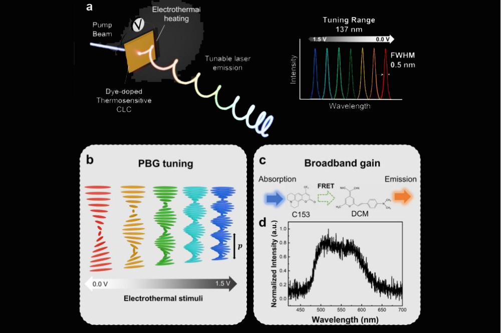
High inversion channel mobility in 1.4 kV vertical GaN MIS-FET
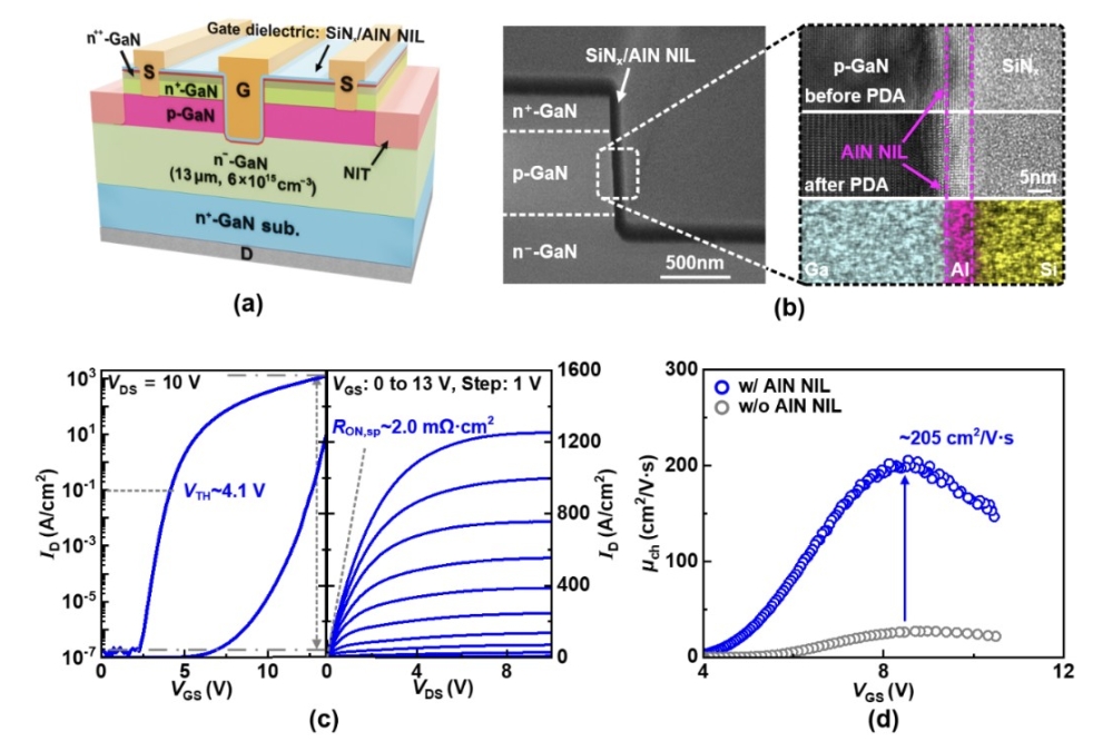
Researchers from University of Science and Technology of China (USTC) have demonstrated a 1.4 kV/2.0 mΩ·cm2 regrowth-free vertical GaN trench MIS-FET with a high inversion channel mobility (μch) of 205 cm2/V·s, which is claimed to be one of the best among the state-of-the-art quasi- and fully-vertical GaN power MOS/MIS-FETs.
The MIS-FET also delivers a normally-off operation with a desirable threshold voltage of 4.1 V and high ON/OFF current ratio (ION/IOFF at -1200 V) of ~108.
1200~1700V power MOSFETs are widely adopted in electric vehicles, photovoltaic inverters and industrial motors. However, for commercially available wide-bandgap semiconductor MOSFETs, the channel resistance (Rch) usually constitutes over 25 percent of the overall specific ON-resistance (RON,sp), due to the relatively low inversion μch (~30 cm2/V·s).
To reduce the conduction loss and enhance power conversion efficiency, it is essential to enhance μch in kilovolt power MOS/MIS-FETs, say the researchers.
The team reports achieving a smooth sidewall and rounded corners in the vertical trench MIS-FET, with optimised gate trench etching. Moreover, they say the high-quality monocrystal-like AlN nitridation interfacial-layer (NIL) has been formed between the p-GaN and SiNx gate dielectric. The AlN NIL can effectively reduce interface trap density (Dit) by approximately one order of magnitude.
The figures above show the (a) Schematic cross section of vertical GaN trench MIS-FET. (b) Cross-sectional SEM micrograph and TEM micrograph of the SiNx/AlN NIL/GaN interface, and distributions of Ga, Al, and Si at the interface. (c) Transfer (left) and output (right) characteristics of vertical GaN trench MIS-FET. (d) Inversion μch of vertical GaN MIS-FETs with and without AlN NIL.
Reference
Zaitian Han, Shu Yang et al., 70th IEEE International Electron Devices Meeting (IEDM) 2025