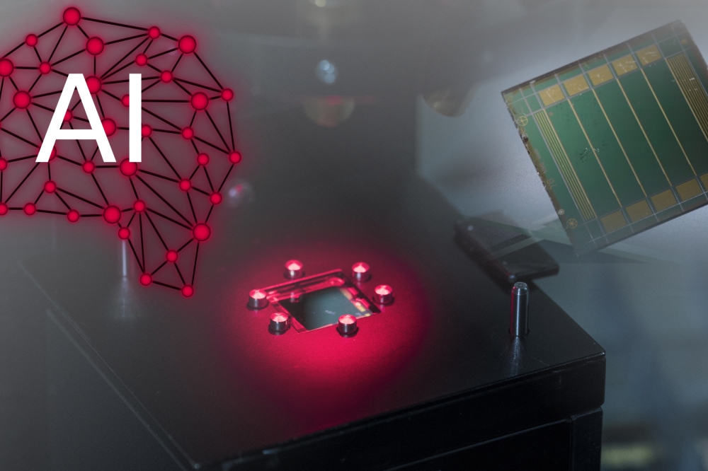


USTC team develops GaN nanowire 'synapse'
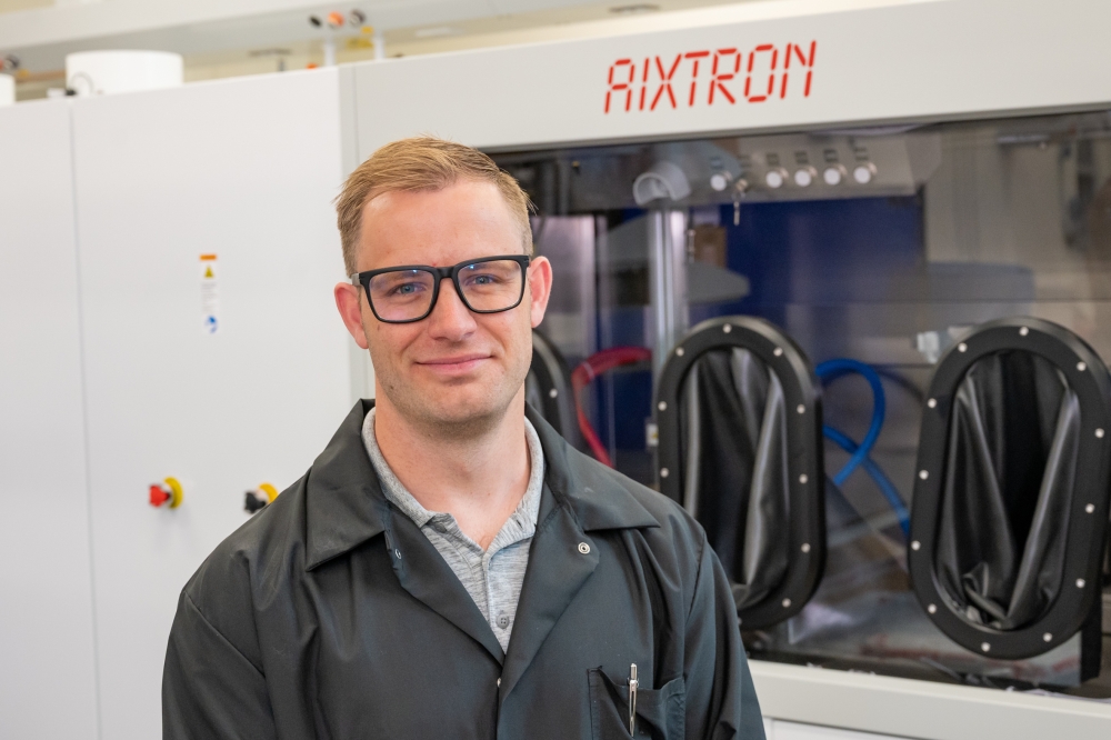
The iGaN Laboratory led by Haiding Sun at the University of Science and Technology of China (USTC) has proposed a novel GaN-nanowire-based photoelectrochemical synaptic devices in a paper published in Nature Communications.
Inspired by biological vision, optoelectronic synaptic devices could be used to integrate perception, information storage, and processing, opening up possibilities for multifunctional sensing systems. However, most optoelectronic synapses rely primarily on physical processes while missing chemical-electric synaptic processes critical for mimicking more realistic brain-inspired functionality.
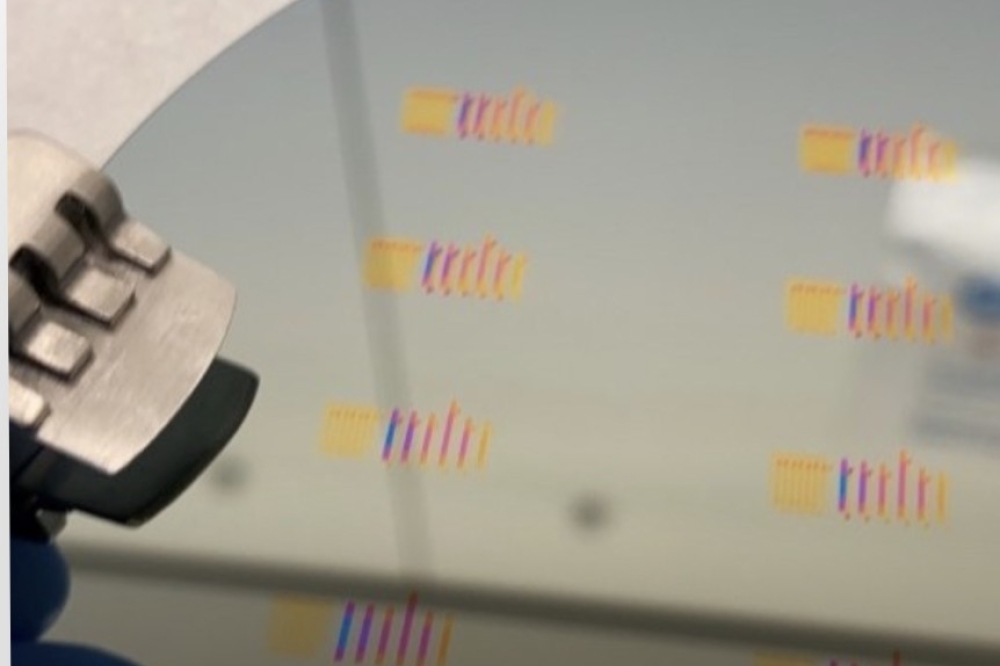
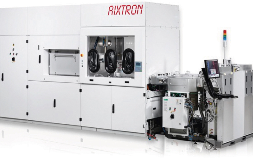
The researchers constructed their photoelectrochemical synaptic device using p-AlGaN/n-GaN semiconductor nanowires and achieved switching between current mode and voltage mode by altering the circuit state, demonstrating both short-term and long-term synaptic plasticity.
By manipulating the semiconductor/electrolyte interface, platinum nanoparticles were decorated on the surface of the nanowires to regulate synaptic response behaviours. They found that the synaptic response of the device was enhanced after the Pt nanoparticles were loaded.
The team say that the device exhibits chemically-regulated synaptic properties similar to biological systems and simulates oxidative stress processes in the human body, including cognitive and visual decline triggered by oxidative stress .
They believe this kind of photoelectrochemical synaptic device could serve as a promising candidate for constructing advanced artificial systems that bridge optoelectronic synapses with biological functionalities.
Reference
Xin Liu, Haiding Sun et al., Nat Commun 15, 7671 (2024)
Secure Your Hydrogen Supply
A study supply of high-purity hydrogen is critical to semiconductor fabrication. Supply chain interruptions are challenging manufacturers, leading to production slowdowns and stoppages. On-site hydrogen generation offers a scalable alternative for new and existing fabs, freeing the operator from dependence on delivered gas.Plant managers understand the critical role that hydrogen plays in semiconductor fabrication. That important job includes crystal growth, carrier gas, wafer annealing, and in the emerging Extreme UV Lithography (EUV) that will enable new generations of devices. As the vast need for semiconductors grows across all sectors of world economies, so does the need for high-purity hydrogen.
Take control with Nel on-site hydrogen generation.
Read more