On the high-frequency frontier with InAlN-based HEMTs
Combining InAlN/GaN HEMTs with GaNOI technology ensures the monolithic integration of high-frequency GaN devices with CMOS technology.
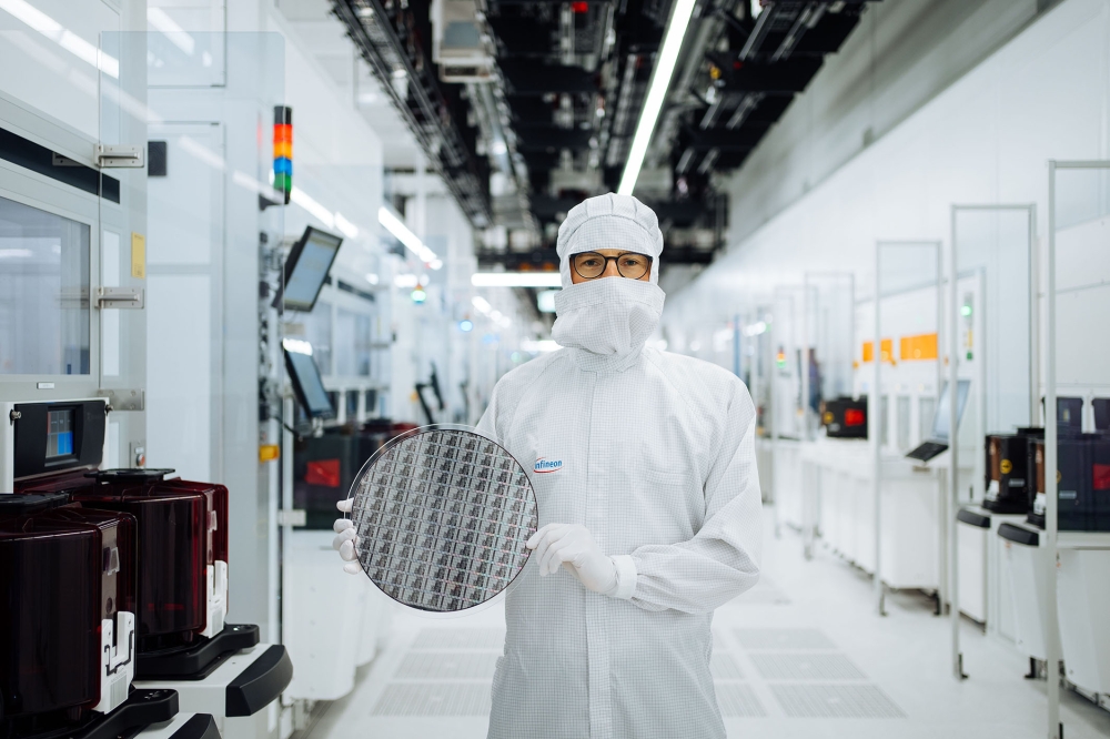
BY HANCHAO LI AND GEOK ING NG FROM NANYANG TECHNOLOGICAL UNIVERSITY, YUE WANG, SHUYU BAO, KENNETH E. LEE FROM SINGAPORE-MIT ALLIANCE FOR RESEARCH AND TECHNOLOGY, HANLIN XIE FROM INSTITUTE OF MICROELECTRONICS, AGENCY FOR SCIENCE, TECHNOLOGY AND RESEARCH, AND EUGENE FITZGERALD FROM MASSACHUSETTS INSTITUTE OF TECHNOLOGY
Within the family of compound semiconductors, GaN is held in particularly high regard. This material is renowned for its many strengths, including its wide bandgap, its high critical electric field, and the high density present in its polarisation-induced two-dimensional electron gas (2DEG).
One device that draws on these merits is the GaN-based HEMT, which outperforms its silicon-based counterpart. Thanks to the robust power-handling ability of GaN, this class of HEMT is well suited to serving in millimetre-wave applications in wireless communication technologies.
While GaN outperforms silicon, it cannot match its maturity. This makes the integration of GaN and silicon CMOS technology attractive, creating a marriage that offers a cost-effective scalable solution by leveraging existing silicon infrastructure while capitalising on GaN’s superior efficiency and thermal stability. However, it is easier said than done. Integration poses notable challenges, particularly in preserving the breakdown voltage and ensuring optimal RF performance.

Figure 1. GaN-on-insulator (GaNOI)-on-silicon wafers are produced by adding an insulating layer between the GaN epilayers and the silicon substrate.
Taking on these challenges, our collaborative team from the Singapore-MIT Alliance for Research and Technology, Nanyang Technological University, and Massachusetts Institute of Technology, is pioneering the use of wafer-bonding technology to enable a GaN-on-insulator (GaNOI) architecture on a silicon substrate.
It’s an effort that’s been underway for several years, with our initial success presented at the VLSI Symposium 2019. At that meeting we reported validation of the enhanced breakdown voltage of the GaNOI structure and its compatibility with silicon CMOS technology.
Our innovative method, described in prior reports, enables the processing of large silicon wafers in standard silicon foundries. Using this approach, we have enhanced device reliability by eliminating the initial transition layer, characterised by a multitude of dislocations and subpar thermal conductivity.

Figure 2. Cross-sectional InAlN/GaN heterostructure schematic showing
the location of the 2DEG and energy band diagram of a GaN
heterostructure.
Another refinement has been substituting the original silicon (111) substrate, which is prone to fragility after high-temperature GaN growth, with a more robust silicon (100) substrate. This switch significantly diminishes the likelihood of wafer breakage during production, leading to increased yield.
More recently, we have started to explore the potential of GaNOI technology in high-frequency applications. By constructing GaN HEMTs on an insulating substrate, GaNOI technology is expected to trim parasitic capacitance and ultimately improve frequency performance.
Typically, GaN-based HEMTs employ either AlGaN, InAlN or AlN as the barrier material. The selection from these three has a great influence on overall device performance and reliability, especially under harsh conditions, such as high temperatures.
The 2DEG that forms at the interface between the barrier layer and GaN lies at the heart of the HEMT, acting as a quantum well filled with high-mobility electrons. Levers for optimising the properties of the 2DEG, such as its density and mobility, include varying the thickness and the material composition of the barrier layer.

Figure 3. Reported fT/fmax values for various GaN-on-silicon HEMT technologies.
Traditionally, AlGaN has been the go-to material for the barrier layer. However, it is not without weakness. A significant downside is the stress induced by the piezoelectric effect, leading to possible lattice defects.
This is where InAlN comes in to play, offering a compelling alternative that’s lattice-matched to GaN, thus minimising strain effects (see Figure 2). Switching to InAlN is the move behind record current-gain cut-off frequencies, which indicate the potential of InAlN/GaN HEMTs in high-frequency applications.
To date, the highest cut-off frequency for AlGaN/GaN HEMTs on silicon substrates is 152 GHz, realised with devices with a recessed gate that have a 75 nm gate length. With this particular device, an AlGaN barrier layer thickness of 25 nm results in 2DEG density of 1 × 1013 cm-2. By replacing this with an InAlN barrier, the thickness of this layer can be trimmed to around 8 nm, while realising an even higher 2DEG density, in the range 1.2 - 1.7 × 1013 cm-2. This improvement is due to a higher spontaneous polarisation for InAlN/GaN, compared with AlGaN/GaN. The thinning of the barrier layer while maintaining a high sheet carrier density is desirable, enabling increased gate modulation control by reducing the gate-to-channel distance, and ensuring an increase in transconductance. With an InAlN/GaN HEMT on silicon, we have recorded values for the cut-off (fT) and maximum oscillation (fmax) frequency of 300 GHz and 400 GHz, for a 30 nm gate length (see Figure 3).

Figure 4. There is much promise associated with the integration of
silicon-CMOS, RF devices and high-power devices, comprising HEMTs on
both III-N and III-As/P layers, on a single wafer forming a hybrid
substrate.
Moreover, in high-temperature applications, InAlN/GaN heterostructures offer unparalleled robustness. At high temperatures, strain effects in the system can become more prevalent, threatening reliability. InAlN is lattice-matched, and thought to provide higher reliability in ultra-high temperature environments, due to the absence of piezoelectric strain.
The improved performance makes it even more attractive to integrate silicon CMOS with high-frequency devices such as GaN HEMTs, and high-power components like power amplifiers (PAs) on GaN layers. Wafer-level integration is a key enabler for developing compact, versatile, and efficient integrated circuits for serving in a wide array of applications, from consumer electronics to advanced communication systems.
Wafer bonding and layer transfer
Wafer bonding has emerged as a promising method for integrating III-Vs onto silicon substrates, a key process for the development of advanced semiconductor devices. Among the various techniques for taking on this task, we prefer fusion bonding, particularly plasma-activated bonding. Its merits include its compatibility with low-temperature processing and the opportunity to use atmospheric pressure conditions. In addition, plasma-activated bonding is able to accommodate materials with mismatches in coefficients of thermal expansion, and is seamlessly compatible with CMOS process technology, making it a versatile choice for diverse semiconductor applications.
The fabrication of our devices began by preparing several sets of wafers, each including: a silicon handle wafer, a 200 mm InAlN/GaN-on-silicon (111) wafer, and a new silicon (100) wafer substrate. A critical initial step was the plasma-enhanced chemical vapour deposition (PECVD) of SiO2 on the front sides of both the silicon handle wafer and the InAlN/GaN HEMT wafer, followed by densification of this oxide. After this, we thoroughly cleaned the surfaces and treated them with plasma activation to promote adhesion, prior to bonding.
Following the first wafer bonding, we turned to grinding and wet etching in an HF/nitric acid/acetic acid solution to completely remove the original silicon substrate. Deposition of 200 nm oxide layers by PECVD on both the GaN HEMT wafer and the silicon (100) substrate followed, prior to densification at 600 °C for several hours in nitrogen gas. The latter step eliminated residual gas molecules and any by-products incorporated into the layer during the oxide deposition. After this densification, we applied chemical mechanical polishing to smooth the PECVD oxide for the second bonding process. The bond strength increased by annealing the bonded wafer pair for 3 hours at 300 °C in an atmospheric N2 ambient (see Figure 5).

Figure 5. Cross-sectional transmission electron microscopy image of a GaNOI wafer.
Scrutinising material quality
We have rigorously evaluated the material quality of our heterogeneous structure with a variety of techniques. According to transmission electron microscopy, our 200 mm GaNOI-on-silicon wafer shows no visible bubbles at the bonding interface, an indication of the high quality of the bonding process (see Figure 6).
Prior to device fabrication, we undertook a comprehensive characterization of our epitaxial wafer, using techniques that included atomic force microscopy, X-ray diffraction, micro-Raman spectroscopy and Hall measurements. Atomic force microscopy provided values for the root-mean-square (RMS) roughness of the wafer surface, while X-ray diffraction and Raman measurements were pivotal in determining the crystallographic structure and quality, providing insights into the strain, defects, and layer compositions of the GaN epitaxial layers. This pair of non-destructive techniques allowed us to evaluate crystalline quality, revealing information about dislocation densities and lattice mismatches, potential obstacles to realising an impressive device performance.
According to atomic force microscopy of a 5 µm by 5 µm area, the RMS roughness of our InAlN/GaN HEMT epilayer on a GaNOI substrate is just 0.7 nm. Such a low value indicates that no significant misfit dislocations are exposed on the top surface.
During the layer transfer processes, the in-plane lattice strain reduced by 5 percent (see Table 1). This could be attributed to the release of stress. Our view is that strain relaxation probably results from diminished elastic strain/deformation, due to the removal of a highly-mismatched silicon (111) substrate.

Figure 6. GaNOI-on-silicon wafer fabrication flow.
Micro-Raman spectroscopy supports this hypothesis, unveiling a significant reduction in compressive stress in the material system, highlighted by a shift in the GaN peak (see Figure 7(b)). Additional evidence for the decline in compressive stress comes from X-ray diffraction measurements. Another insight provided by Raman spectroscopy is the extent of stress within the GaN channel. According to simple calculations based on the shift in the Raman wavenumber, there is a reduction in stress of 0.1 GPa after layer transfer, associated with a reduction in strain in the GaN epilayer.
The reduction in stress resulted in increases in the 2DEG mobility and the concentration of carriers within the InAlN/GaN heterostructure. Note that similar observations have been reported by Cosmin Romanitan and colleagues at the National Institute for Research and Development in Microtechnologies, IMT Bucharest.
We have also undertaken room-temperature Hall measurements to determine the carrier concentration, mobility, and sheet resistance for both our GaN-on-silicon and GaNOI-on-silicon wafers. These results, presented in Table 2, reveal that after substrate replacement, the mobility of the
In0.17Al0.83N/GaN heterostructure increases from 930 cm2 V-1 s-1 to 1380 cm2 V-1 s-1 and the 2DEG density slightly decreases from 1.97 × 1013 cm−2 to 1.89 × 1013 cm−2, leading to an improvement in sheet resistance from 301 to 284 Ω/square. These gains translate into an enhanced performance for our GaNOI-on-silicon devices.

Figure 7. (a) Atomic force microscopy of InAlN/GaN on a GaNOI-on-silicon substrate and (b) Raman spectra of both GaN-on-silicon and GaNOI-on-silicon samples, high resolution E2 modes.
Device evaluation
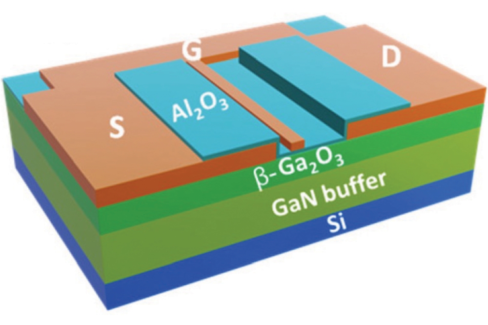
Using a standard fabrication process flow, we have fabricated GaN HEMTs from a small piece of a 200 mm InAlN/GaNOI-on-silicon wafer, using inductively coupled plasma-reactive ion etching with a
Cl2-based plasma to realise device mesa isolation. We formed ohmic contacts using a Ti/Al/Ni/Au metal stack annealed for 30 s at 775 °C. According to linear transmission line model analysis, ohmic contact resistance is 0.21 Ω-mm. To complete transistor fabrication, we formed Ni/Au T-shape Schottky gates, with a gate foot length of 120 nm, a head length of 500 nm and a stem height of 170 nm.

Table 1. Comparison of key X-ray diffraction parameters.
Here we report current-voltage (I-V) and RF measurements of devices with a 2 × 20 μm gate width, and gate-source and gate-drain distances of 1.5 µm. Saturation current density peaks at 1.28 A mm-1, for a gate-source voltage of 2 V, and on-resistance is 2.3 Ω·mm (see Figure 8(a)). Transfer characteristics included a peak transconductance of 320 mS/mm and a threshold voltage of - 3.9 V (see Figure 8 (b)).
Additional measurements reveal a Schottky gate barrier of 0.81 eV, and an off-state gate leakage current of about 117 μA mm-1 at -10 V (see Figure 8(c)). This indicates no apparent electron tunnelling through the barrier layer, despite the highly localised electron density near the gate.

Table 2. Hall parameters for wafers pre- and post- bonding.
We also plotted semi-log-scale transfer curves for a drain-source voltage of 1 V (see Figure 8(d)). Under reverse bias, we determined an on-off ratio for the current of the GaNOI device of 2.6 x 10⁶ and a subthreshold slope of 89 mV dec-1. These values confirmed that our devices offer good gate control.

Figure 8. (a) Output and (b) transfer characteristics of a 120-nm gate
GaNOI device. (c) Gate leakage characteristics and (d) semi-log-scale
transfer curves at Vds = 1 V.
To evaluate the high-speed capability of our HEMTs, we measured their current gain (|h21|2) and maximum available gain/maximum stable gain, using measurements up to 40 GHz (see Figure 9 for details). We obtained peak values for fT and fmax of 96/87 GHz and 96/101 GHz by extrapolating from the current gain (|h21|2) and the maximum available gain/maximum stable gain with a -20 dB/dec slope.

Figure 9. RF small-signal characteristics of a GaNOI device
at (a) Vds = 5 V and Vgs = -3 V and (b) Vds =
10 V and Vgs = -3 V, with the pad parasitics de-embedded.
Benchmarking our devices with GaN-on-silicon HEMTs using a figure of merit that’s the product of fT and the gate length determined that our device is comparable to the state-of-the-art. This underscores the great potential for improving high-frequency performance with GaNOI technology, with GaNOI-on-silicon offering much promise for future millimetre-wave applications. We have no doubt that this technology will be able to meet the demands of future advanced wireless communication systems, and open up new possibilities in high-frequency electronics.

Figure 10. Comparison of the fT of GaNOI and GaN HEMTs, both produced on silicon substrates.