UV LEDs go micro
Shrinking UV LEDs to a micron or so delivers multiple benefits, including higher efficiencies and opportunities in new applications.
BY JENS RASS FROM FERDINAND-BRAUN-INSTITUT FBH, BERLIN
Many applications can be served by the UV LED, including disinfection, sensing, and material processing. For this class of device, sources emitting within the far-UVC at wavelengths below 240 nm are attracting considerable attention, as they have the potential to deactivate pathogens without damaging human skin. However, the uptake of the UV LED is being held back by its efficiency – it is far lower than its siblings that emit visible light.
For those visible emitters, over the last few years much effort has been directed at scaling dimensions, with the diameter of the LED reduced to below 100 mm, and sometimes shrunk to less than 10 µm. Motivating this miniaturisation is the creation of light-emitting pixels for display technologies, such as augmented- and virtual-reality headsets.
Our research team at the Ferdinand-Braun-Institut FBH, Berlin, has brought these two worlds together by developing UV microLED arrays. This format offers two substantial advantages over conventional UV LEDs with large emitter areas: a higher efficiency, thanks to enhanced light extraction; and the opportunity to create individually addressable emitter arrays, which can generate temporarily and spatially modulated UV radiation patterns. A number of applications could benefit from these arrays, including material processing, mask-free photolithography, sensing, non-line-of-sight communication, and UV-fluorescence microscopy.
One issue that plagues LEDs emitting in the far-UVC is a fairly low emission efficiency. Typical values for external quantum efficiency (EQE) and wall-plug-efficiency are below 1 percent, due to a number of factors that include strong non-radiative recombination of charge carriers, a low injection efficiency, and a low light-extraction efficiency. For the latter metric, values are 10-20 percent for LEDs emitting in the UVB and UVC, and fall to about 5 percent for those that emit in the far-UVC.
The main reason for the poor light extraction efficiency is the high degree of total internal reflection at interfaces. The trapped light is subsequently absorbed in various layers of the LED chip (see Figure 1).

Figure 1. UV LEDs have a low light extraction efficiency (LEE), due to the trapping of photons in the chip and subsequent absorption within the device structure, including layers of GaN, metals, and insulators. Light trapping is more severe in far-UVC LEDs, since more transverse-magnetic polarised light is travelling in the quantum well plane.
For UVB and UVC LEDs, the light that’s generated in the AlGaN-based layer structure is emitted through the transparent substrate. In most cases this is sapphire, which has a refractive index in the UVC of 1.8 - 1.9. As the AlGaN stack has a refractive index of approximately 2.7 and the surrounding air a value of 1, only radiation within a small angular range can leave the chip. Consequently, most of the photons that hit the AlGaN-sapphire and sapphire-air interfaces do so at angles beyond the critical angle for total internal reflection, causing them to be trapped inside the chip. Since many of the materials typically used to make the LED are inevitably absorbing – light can be absorbed at the metal contacts, the GaN p-side contact layer, and sometimes the insulators – there is a low probability for photon emission after several reflections.
Unfortunately, the likelihood that light is trapped within an LED increases at very short UV wavelengths. Reaching this spectral domain requires an increase in the aluminium mole fraction in the active region of the AlGaN quantum wells. This leads to a re-ordering of the valence subbands, resulting in a switching of the optical polarisation of the generated photons from dominantly transverse-electric, with the electric field vector lying in the chip surface and the photon emission perpendicular to it, to transverse magnetic. Since light polarised in the transverse magnetic direction is emitted parallel to the chip surface, the majority of photons traverse with a direction outside the light escape cone, and thus have a very high probability of undergoing total internal reflection and subsequent absorption.

Figure 2. Light extraction from the UV microLED is enhanced by internal
reflection at the mesa side wall and redirection towards the chip back
surface. This requires small mesas with slanted and highly reflective
side walls and small diameters.
Increasing the light-extraction efficiency is a common goal for all developers of LEDs. For devices emitting in the visible and UV, improvements come from introducing surface patterning, reflective contacts, and encapsulation techniques. However, it’s far from easy to enjoy success with these approaches with the UVC LED. Progress is held back by strong absorption and instability of materials under irradiation with high photon energies.
Getting the right angle
Our approach is to pattern the surface of the AlGaN-based LEDs into arrays of individual micro pixels with a slanted mesa side wall. With this architecture, photons emitted parallel to the chip surface are redirected towards the chip backside where they can be extracted (see Figure 2). To optimise performance, the micro pixels need to have a small diameter and smooth, reflective sidewalls with an angle near 45 °.
To fabricate these emitters, we began by growing LED layer structures made of AlGaN on 2-inch sapphire substrates by MOCVD. The active region in these epiwafers is designed to deliver single peak emission at 233 nm.
We patterned the wafer surface by photolithography and employed chlorine-based plasma etching to create circular mesas with diameters between 1.5 µm and 100 µm and a sidewall angle of 45 ° to 50 ° (see Figure 3). While this step proved to be very challenging, it is crucial for guaranteeing a high efficiency through the re-direction of transverse-magnetic polarised photons. Our work involved having to fine-tune the parameters for the photolithography process on the transparent and heavily bowed wafers, and developing suitable plasma etch conditions, including the gas mixture, plasma power, and pressure.

Figure 3. The mesa definition is a crucial step in the production
process, in particular the adjustment of the sidewall angle, as well as
the alignment of the following layers.
Following etching, we deposited and annealed p- and n-metal contacts. In order to realise a high reflectivity at the tilted mesa surface, we then deposited a SiO2 layer. This electrically insulating oxide is fully transparent in the entire UV range, and offers a high refractive index contrast to AlGaN, enabling it to act as a reflector. We capped the SiO2 with aluminium, also acting as a reflector, before adding thick metal pads for an electrical contact.
The final processing steps involved dicing LED chips from the processed wafer and mounting them on ceramic submounts in a flip-chip geometry. For comparison, we also produced LEDs that incorporate a different insulator, by replacing SiO2 with SiNx. Since SiNx has a smaller refractive index contrast to AlGaN and absorbs in the UVC range, LEDs with this insulator should not provide a significant enhancement in light extraction.
Miniature marvels
Measurements of the electroluminescence characteristics of our devices, using an integrating sphere, reveal that the micro pixel architecture produces a very strong increase in output power, and therefore efficiency. Moving from a conventional design to a pixel diameter of just 1.5 µm produces a fourfold hike in peak EQE (see Figure 4). Scaling to such small dimensions is needed to benefit from miniaturisation – there is no benefit for only reducing the LED diameter to 5 µm. Note that this is not the case with visible microLEDs, where benefits are already realised for devices with diameters of 10 µm or even more. What’s more, for our devices the peak EQE occurs at current densities between 70 A cm-2 and 200 A cm-2, while for LEDs in the literature, the record peak EQE tends to occur at very low current densities that are unsuitable for applications.

Figure 4. Left: The peak EQE is drastically increased by reducing the
diameter of the micro pixels due to increased light extraction. Right:
UVC LED chip with standard large area chip layout mounted in flip-chip
geometry on a ceramic submount.
Another noteworthy attribute of our UVC emitters is that their improvement in light extraction efficiency does not saturate at small mesa diameters. In sharp contrast, for microLEDs in the visible range – and especially those emitting in the green and red – there is a strong reduction in the EQE at small diameters. This fall in efficiency is attributed to non-radiative recombination of charge carriers at defects at the plasma-etched mesa side wall. As we do not see such an effect, we can conclude that any possible increase in losses must have been more than compensated for by the improvement in the light extraction efficiency.
This is further confirmed by the LEDs that employed the SiNx insulator: The emission power was not significantly enhanced for small diameter structures since the refractive index contrast to AlGaN was too low to achieve total reflection, but neither did the efficiency drop for the small diameters, as would be seen if nonradiative carrier recombination at the mesa sidewall was an issue.
Our 233 nm microLEDs produce a record peak EQE of 1.6 percent and a wall-plug efficiency of 0.88 percent. Output powers are 1.7 mW and 3.5 mW at 20 mA and 50 mA, respectively. While these values are lower than those for LEDs emitting in the visible, UVB and near-UVC, they are the highest numbers currently reported. That makes our progress a significant step towards bringing far-UVC LEDs closer to deployment in practical applications, such as nitrogen oxide gas sensing and skin-safe eradication of pathogens.
We are now working on further improvement to the efficiency and output power of our far-UVC LEDs. Our investigations include improving the AlN-sapphire templates, the AlGaN-LED heterostructure, and the microLED chip process. By packing pixels more densely, adding additional layers for efficient current spreading, and using strain engineered templates to enhance transverse-electric polarised optical emission, we have already realised our first promising results, with EQE increasing to peak values of up to 2.9 percent.
These improvements in the efficiency of far-UVC LEDs, resulting from an increased light extraction efficiency, are important for the realisation of high-power emitters. However, it’s important to not overlook a number of other interesting opportunities connected to this technology.
One of these is to combine our UV LED, patterned into electrically separated pixels, with a matrix- or CMOS driver chip. It’s a marriage that creates UV light engines and UV micro displays that can serve in many new applications. For example, the spatially and temporarily modulated light pattern generated by such a device could illuminate the photoresist on wafers, thereby creating a mask-free lithography system. Such a source of UV emission could also be deployed for rapid prototyping and 3D printing/patterning. Opportunities also exist in the life sciences, with arrays of UV microLED pixels providing the light source for DNA fluorescence spectroscopy and other sensing applications.

Figure 5. A UV micro-LED array with pitch of 2 µm and a pixel diameter of 1.5 µm emitting at a wavelength of 300 nm. Light microscopy image (left) and scanning electron microscope image during the production process (right).
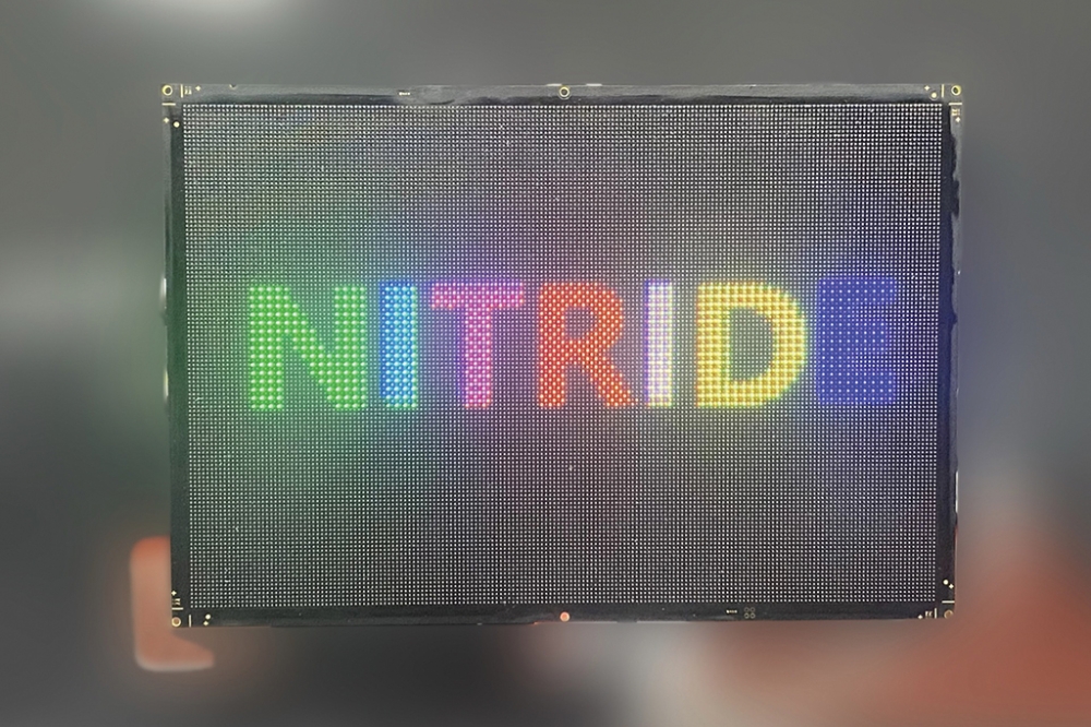
It’s also worth noting that our technology is not restricted to the far-UVC. It can also be applied to nitride-based LEDs emitting in the UVC, UVB, and all the way to UVA, opening up a large number of applications.
In order to demonstrate the feasibility of such an approach, we have developed a chip emitting at 300 nm that emits our FBH-logo (see Figure 5). While the device cannot yet change its pattern, it illustrates the potential of UV microLED technology.