P-GaN gate HEMTs have record threshold voltage
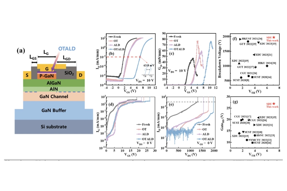
Researchers at Shandong University in China have reported an enhancement-mode P-GaN/AlGaN/GaN metal-insulator-semiconductor HEMT (MIS-HEMTs) by combining thermal oxidation treatment of P-GaN with atomic layer deposition (OTALD) prior to gate metal deposition.
This increased threshold voltage significantly to 7.1 V, with improved gate breakdown voltage and off-state breakdown voltage of 26.9 V and 1980 V respectively.
Low activation rate of Mg dopants in P-GaN typically results in the threshold voltage less than 2 V without additional processing, limiting the application of P-GaN/AlGaN/GaN HEMTs in high gate voltage drive circuits. In response, the researchers applied an integration of oxygen annealing treatment (OT) of P-GaN and atomic layer deposition (ALD) technology.
Device fabrication began with the P-GaN cap layer etch and mesa isolation. The ohmic contacts were then formed via magnetron sputtering and annealing in N2 atmosphere. After depositing SiO2 passivation layer, the opening of the gate region was patterned by inductively coupled plasma (ICP) etching.
Fabrication of the MIS structure on the opening of the P-GaN gate region by OTALD technology started with the thermal oxidation treatment. Followed by a 5 nm Al2O3 dielectric layer deposition by plasma enhanced atomic layer deposition (PEALD) process. Finally, gate metal stack was deposited by magnetron sputtering to form the gate metal field plate. The untreated fresh P-GaN gate HEMTs were fabricated as references.
Atomic force microscopy (AFM) measurement shows decreased surface roughness after oxygen annealing treatment process, indicating that this process produces a flat oxide layer on the P-GaN surface and effectively removes other contaminants. Cross-sectional HRTEM presents a dense and smooth oxide layer is formed. The presence of this oxide layer provides a gradually-varied transition between Al2O3 and P-GaN, leading to a significantly improved interface quality between these two materials.
Figure: AFM-measured P-GaN surface profiles (a) before and (b) after OT process. Cross-sectional HRTEM image of the MIS contact of (c) ALD-HEMTs and (d) OTALD-HEMTs.
Owing to the higher gate Schottky barrier of oxide layer and the voltage division effect of the dielectric layer, OTALD-HEMTs present increased threshold voltage significantly from 1.8 V to 7.1 V compared to conventional P-GaN gate HEMTs, with a minimal hysteresis of 63.8 mV and high on/off current ratio above 108. Smooth interface of the oxide layer can reduce the scattering of the 2DEG within the channel, contributing to a higher transconductance (75.9 mS/mm, an increase of 63%).
The dense oxide layer possesses a wider bandgap and higher thermodynamic stability than P-GaN, which is less susceptible to degradation caused by hot electron bombardment and suppress gate leakage current. And the presence of the dielectric layer beneath the gate can reduce surface states and fill defects on P-GaN surfaces, decreasing leakage current and suppressing hot carrier effects. Thus, the OTALD-HEMT further enhanced the forward gate breakdown and off-state breakdown voltage to 26.9 V and 1980 V, a 42 percent and 51 percent improvement compared to the conventional P-GaN gate HEMT.
Future research will focus on achieving the variation of threshold voltage within a certain range through different dielectric layer thickness in OTALD technology.
The figures above show: (a) Schematic cross section of OTALD-HEMTs. (b) Transfer and (c) transconductance characteristic of four types of P-GaN gate HEMTs. (d) Gate breakdown and (e) off-state breakdown characteristics of four types of P-GaN gate HEMTs. Comparison for (f) gate breakdown and (g) off-state breakdown with different threshold voltage between this work and other studies.
Reference
Siheng Chen, Peng Cui et al, High Breakdown Voltage P-GaN Gate HEMTs With Threshold Voltage of 7.1 V, IEEE Electron Device Letters, vol. 45, no. 12, Dec. 2024

