
IMiF expands GaN research capability with Samco ICP-RIE Platform
IMiF strengthens its GaN research infrastructure with the addition of a Samco ICP-RIE platform, enabling more advanced development of next-generation wide bandgap power devices.
Samco Inc, a manufacturer of semiconductor processing equipment, has announced that Łukasiewicz – Instytut Mikroelektroniki i Fotoniki (Łukasiewicz – IMiF) in Warsaw, Poland, has selected Samco plasma processing systems to support the development of next generation GaN power devices.
The acquisition of the systems is funded under Poland’s National Recovery Plan, supporting Łukasiewicz – IMiF in strengthening its research infrastructure in areas of strategic importance to the modern economy. The Institute is expanding its laboratories and equipping research teams with advanced instruments for microelectronics, photonics, and advanced materials. The investment strengthens technological capabilities, enabling the delivery of applied R&D projects with strong industrial relevance and reinforcing the Institute’s role in translating high quality research into tangible economic impact. In addition, the installation will enhance Łukasiewicz-IMiF process capabilities for AlGaN/GaN HEMT and vertical GaN trench MOSFET device development as part of the European WBG Pilot Line initiative funded by Chips Joint Undertaking (Chips JU).
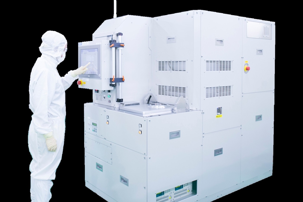
To support its GaN R&D activities, Łukasiewicz-IMiF selected the RIE-400iP ICP-RIE plasma etching system, along with the RIE-10NR reactive ion etching system, and the UV-1 UV ozone surface treatment system. The tools were selected through a public tender process in collaboration with partner company Electron-mec and are scheduled for delivery by the end of June 2026.
Dr. Andrzej Taube, Leader of the GaN-Based Devices Area at Łukasiewicz – IMiF, commented, “The expansion of our plasma etching and surface treatment capability is a key step in establishing the GaN pilot line at Łukasiewicz-IMiF. Advanced control of AlGaN/GaN etching processes is essential for the development of high-performance HEMT and vertical GaN MOSFET devices. The selected systems will support both research-scale innovation towards industry deployment to strength country economic resilience via realization of Poland’s National Recovery Plan and as well as pilot-line process development within the WBG Pilot Line framework.”
The RIE-400iP will serve as the primary platform for GaN and Ga2O3 etching. In addition to standard ICP-RIE capability, the system supports atomic layer etching (ALE), enabling controlled, low-damage etching of AlGaN/GaN heterostructures. Precise control of etch depth, sidewall smoothness, and vertical profile is critical for state-of-the-art GaN power device fabrication, where interface quality and structural accuracy directly impact device performance and long-term reliability. The system is also equipped with two interferometric endpoint monitor units to support accurate layer thickness control during complex etching processes.
The RIE-10NR system will provide dedicated capability for SiO2 and SiNx etching, supporting dielectric processing steps within GaN device fabrication flows. The UV-1 benchtop UV ozone cleaner will be used for precision surface preparation and organic residue removal, contributing to improved process integration and device consistency.
“We are honored to support Łukasiewicz-IMiF in its GaN power device development,” said Tsukasa Kawabe, President and COO of Samco Inc. “Wide bandgap semiconductors such as GaN are central to next-generation power and RF electronics. Plasma etching technologies with advanced process control, including ALE capability, are increasingly important for achieving the precision and reliability required in modern GaN device fabrication. Samco remains committed to contributing to Europe’s semiconductor ecosystem through collaborative research and technology development.”
The three systems will be installed at Łukasiewicz-IMiF facility in Warsaw, strengthening its role within the Łukasiewicz Research Network, one of the largest research organizations in Europe, and enhancing Poland’s contribution to European wide bandgap semiconductor development.


