Aixtron looks to ‘go large’
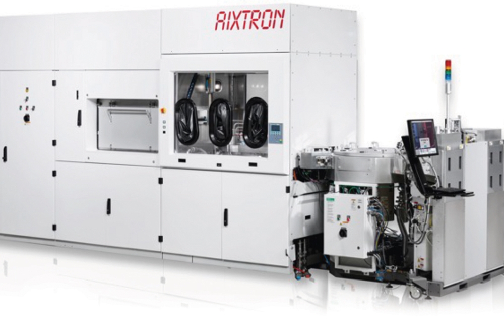
Supporting the shift to production with larger
wafers is Aixtron, the world’s leading manufacturer of MOCVD tools,
explains the company’s VP technology Jared Holzwarth.
AN INTERVIEW WITH RICHARD STEVENSON, EDITOR, CS MAGAZINE
RS: Back in 1995, when Compound Semiconductor premiered, Aixtron had already celebrated its tenth anniversary. How does the Aixtron of 1995 compare to how it is today?
JH: Well, I was 17 back in 1995, so I’m not completely sure how it was in ‘95! But I do know that Aixtron is very much the same in some ways, and in other ways it’s a bit different.
What has been the same is the innovative spirit. From its inception, Aixtron’s been based on innovation and a desire to challenge the impossible.
Where I think it’s changed significantly is how much closer we are to the customer, in terms of process, application, and know how. While we were putting all our focus on delivering performance hardware in the past, today we’re looking at turnkey solutions that are closely co-optimised with the customer, to make sure they’re successful in all their milestones. I think you can see the results of that with the latest silicon carbide MOSFETs and GaN HEMTs. They really show that new side of Aixtron.
RS: In the late 1990s, the GaAs microelectronics sector dominated high-volume manufacturing within the compound semiconductor industry. Since then, we have seen the growth in sales of GaN LEDs, and more recently wide bandgap power electronics. Aixtron began with MOCVD tools for traditional III-Vs, such as GaAs and InP. How difficult has it been to expand into the nitrides and silicon carbide?
JH: For the nitrides it went in two waves of technology adoption. We developed dedicated solutions for each of those big waves.
For the solid-state lighting push – back at that time, I was actually at a customer of Aixtron, Philips Lumileds – the main focus was associated with the temperature control on each substrate, how that occurred over all the substrates, and how to do that for longer deposition campaigns. We developed a technology with closed-loop temperature control to manage temperatures at the wafer level. With the adoption of 4-inch, at the time of our launch of a G3 platform, higher volume manufacturing started to begin.
The second wave was more focused on GaN-on-silicon structures for power devices. That was more than ten years ago. Here we faced one crucial problem: when we started to grow GaN-on-silicon, it would result in gallium melt-back etching of the silicon substrate, if we didn’t have a completely clean reactor. It was a critical point for us, because we were just undertaking development of the very first cassette-to-cassette wafer automation for our MOCVD systems aiming at a full automation for the planetary reactor design. Exchanging any reactor parts between runs, like the covers that protect the reactor walls from getting coated, wouldn’t be suitable for volume manufacturing, reliability or cost wise. We took a strategic decision to develop in-situ clean technology, which is one of our fundamental technology building blocks since then. It has helped all of our customers master the complex requirements of GaN-on-silicon epitaxy and volume production.

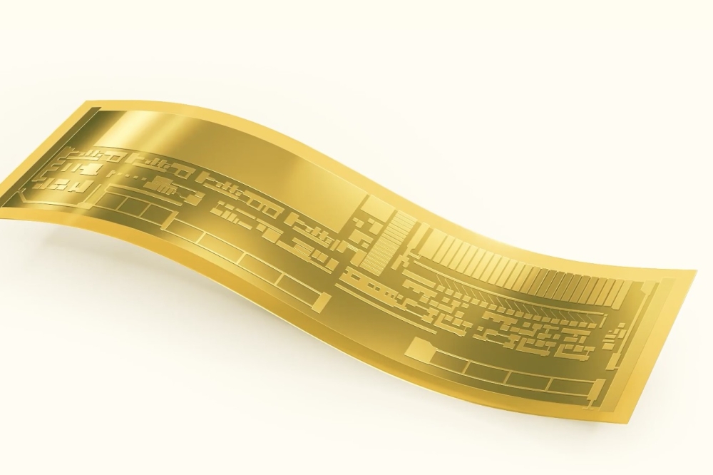
Photoluminescence map of a highly strained AlInGaAs multi-quantum-well
on a 150 mm InP wafer. The average value is 1536 nm, and the standard
deviation, for a 5 mm exclusion zone, is 0.77 nm.
For GaN-on-silicon power devices to succeed, we had to grow highly uniform HEMT structures on silicon substrates, at the time 150 millimetre. It was a big challenge because of lattice mismatch. There was a lot of work that went into managing the strain, to prevent slip lines and edge cracks. At that time, we introduced a curvature sensor to our tools, which really changed the life of process engineers, allowing them to measure and monitor strain build up throughout epitaxy growth in real-time.
For silicon carbide, we’ve been involved for more than 20 years. We took a big turning point in the last four years, when we really framed a key technology question that plagued us for years. That was: What drives the edge effect or the doping profiles that prevents us from getting even better uniformities?
The team I worked with on this was really amazing. Their dedication and efforts to solve this key question, what drives that edge effect, led them to innovate what we call Multi-Ject technology. This solution allowed us to achieve record uniformities on both 150- and 200- millimetre substrates, ahead of what you can get on single wafer tools, and expand rapidly in the silicon carbide market.
RS: In the 1990s you launched your first Planetary reactor. Is this advance, allowing the growth of multiple wafers, arguably the biggest milestone in Aixtron’s history?
JH: It certainly set the direction for Aixtron’s development for many years to come. However, I would say the close-coupled shower head, which we brought into our portfolio from the Thomas Swan Scientific Equipment Division acquisition – known today as Aixtron Limited – had an equal part to play. Both technologies are fundamental to our success. The Planetary Reactors are our workhorse for 150- and 200-millimetre substrates, allowing the platform to secure the lowest possible cost-per-wafer while achieving single-wafer uniformities. The Showerheads are shining for the larger configurations, in the 300-millimetre product offerings.

The aluminium composition range of the AlGaN barrier across a 200 mm
GaN-on-silicon epiwafer, in absolute terms, is below 0.5 percent.
RS: Over many decades Aixtron has seen cycles of growth and periods of contraction. Obviously, any manufacturer would prefer steady growth in the market it serves. What strategies have you adopted to support rapid growth, followed by quieter times?
JH: We had to change things after the first LED investment wave. We ended up diversifying our offerings, to decrease our dependency on a single application. At that time, our revenue was mostly driven by sales of equipment to be used for gallium nitride LEDs. Now, because of that diversification, we’re serving GaN-on-silicon power markets, silicon carbide power markets, telecom and LEDs. This has resulted in dampening out a lot of ups and downs. The diversification also allows us to keep a more steady demand across different applications, while leveraging synergies between them.
We also work closely with our suppliers and supply chain to ensure we can ramp up on time when our customers want more volume for the next market push.
In particular, now with serving the power device end market and inherently the automotive OEM, we were prepared for a potential demand hockey stick and we took great pride in being able to deliver the volumes our customer needed in the last year with the rapid demand growth in GaN and SiC power.
RS: The progress of the compound semiconductor industry can be seen in the increase in substrate size. Your company talks about this, using the phrase ‘Going large’. You feel that the first application to really embrace this concept is 200-millimetre GaN power devices. How has Aixtron supported this move?
JH: The shift to larger wafers is typically stirred in one of two ways. One way is when the volume within one application is large enough that going to the next wafer size can bring a strong advantage – not only in the epitaxy, but back-end cost reduction. Creating a reduction of 30 percent per area is usually the driving factor.
The other driver for large size is technology. Going to a larger wafer allows you to access more refined back-end equipment that has better accuracies or smaller line widths.
Our mission is to just develop the optimum solution whenever the customer needs us to, whether it’s 150, 200 millimetre, et cetera. We’re the first to enable cassette-to-cassette automation for MOCVD, and that includes the in-situ clean technology I mentioned earlier. We are still the only one combining this for volume production with large 200-millimetre batch solutions. Furthermore, to support our customer needs, our latest 200-millimetre products all embark on loading wafers through SMIF front-end access, in order to ensure minimum handling and improve particle performance while reducing the cost of the fab. This is an example of how ‘Going large’ helps you at multiple levels in your production.

The aluminium composition range of the AlGaN barrier across a 300 mm
GaN-on-silicon epiwafer, in absolute terms, is below 0.4 percent , in
line or better than 200 mm performance.
RS: Recently, Infineon grabbed the headlines for developing processes to produce GaN power devices on 300-millimetre silicon. We have also seen companies like Aledia touting 300-millimetre GaN plans for microLEDs. In terms of volume production, what do you think will be the next device to ‘go large’?
JH: It’s a good question. To start, large is a bit relative. For the growing indium phosphide photonics market, for example, 150 millimetres is a really big leap for them, mostly driven by the increase in demand. We are ahead in the solution space for that as well. We have already ported over our learnings from gallium nitride developments, in order to enable full cassette-to-cassette wafer automation with in-situ clean technology for our arsenic-phosphide platform, which we call the G10-AsP.
For gallium nitride, we were the first developing production tools for a 300-millimetre ramp up. We believe the lower-breakdown-voltage devices are ideal candidates for this. We see plenty of applications, including powering advanced AI GPUs.
We’re working very closely with customers to share the benefits from all process and device know-how we’ve acquired in the 150- and 200-millimetre evolutions to ensure a smooth transition towards 300-millimetre.
MicroLED is another application that will be a potential candidate for 300-millimetre. That is mostly driven by the need for a very small pixel size – one micron or less. Not every customer will shift to 300-millimetre, though some applications will. We see that as a benefit, based on our introduction into 300-millimetre GaN-on-silicon.
RS: Another exciting piece of news from late 2024 came from SICC, which produced the first 300-millimetre SiC substrate. What is your view on potential 300-millimetre demand for SiC?
JH: Yes, it was exciting to see this first wafer, considering that 200-millimetre substrates are just recently being put into mass production for silicon carbide power devices. We are well aware that it will take quite a few years for the wafer to be cost-attractive for our customers, but at the same time, we are making sure the right epi solutions will be there when they are needed.

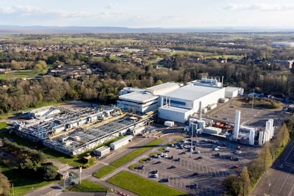
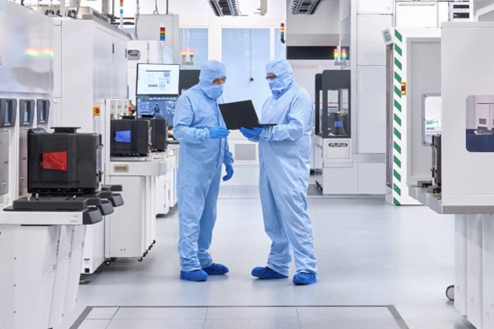
Aixtron’s recently opened Innovation Centre.
RS: In general, what are the challenges in developing reactors that can produce 300-millimetre substrates? And when working with this larger size, what are the pros and cons of using single-wafer and multi-wafer tools?
JH: As a matter of fact, we did deliver our first 300-millimetre reactors for compound material in 2006. At the time, indium gallium arsenide was the ideal candidate to replace silicon as a channel material for advanced CMOS. We did engineer the first fully automated 300-millimetre MOCVD tool for compound customers, with systems installed all over the world at leading IDMs or foundries.
Generally, there is no fundamental challenge to developing reactors, in relation to substrate size. We have two core technologies in our portfolio, and depending on specific application requirements, we will shape the ideal product for our customers.
Our GaN power transition from 200- to 300-millimetre has been surprisingly smooth. We were able to show similar performance on 300-millimetre within months of starting up our development programme.
We don’t see technology segmented solely on single-wafer versus multi-wafer tools. In particular, we have proven over many years that with our Planetary technology, using a single-wafer approach while being a batch, we have the benefit of both worlds. In the end, we use batch in order to have good cost-effectiveness. We believe that single-wafer ‘control’ is needed for improved uniformities. In the end, your volume and your individual application requirements will determine whether you select a single-wafer architecture or a batch-wafer reactor.
RS: During the history of Compound Semiconductor, there has been an expansion in the range of materials used to produce devices. Over the last decade, gallium oxide has emerged as the new kid on the block. What’s your view on this ultra-wide bandgap semiconductor, and how are you supporting its development?
JH: At Aixtron we’re always eager to work on new materials and challenges. We’ve been involved in gallium oxide since the beginning, having our Close Coupled Showerhead R&D reactor systems placed across leading universities to respond and innovate on these new emerging materials. I think the interest in gallium oxide has been growing for many years, predominantly coinciding with improvements in substrate technology and improvements in epitaxy performance.
While we see this improving year after year, we anticipate that it will take time to get to volume production. A lesson learned from GaN-on-silicon is that the power market is relatively conservative with new materials. A certain number of players needs to be in place to ensure the full ecosystem is ready to focus and take advantage of the new material. We anticipate the first product for gallium oxide may be launched in a few years, but it is likely that volume production will be more in the next decade.
RS: You have just opened the Innovation Center. What is the motivation behind this move, and what do you hope its addition will do for the progress of Aixtron?
JH: We’re extremely proud of our new Innovation Center. It opened in December 2024 at the company’s headquarters in Herzogenrath, Germany. I can confirm our first tools are rolled in, and we are already processing first wafers.
The motivation for us was really the upcoming move to 300-millimetre, driven by space constraints and by the vision to engage even deeper with our customers in our lab to develop solutions for their need. We’re always pushing the application limits, and to do so, we needed the Innovation Center.
This new research and development complex with 1,000 square metres of cleanroom space lays the perfect foundation for the transition to 300-millimetre wafer size.
Our executive board decided to invest in the future and really did a great job making that happen quickly. The groundbreaking ceremony and start of construction was in November 2023. One year later we are already celebrated the opening. What it means for us is really setting up ourselves for success in the decade to come. We’re excited that compound semiconductors are going mainstream and entering into 300-millimetre fabs around the world, and we are ready to have the infrastructure to make that transition a success for our customers.

Aixtron’s VP of Technology, Jared Holzwarth.