

GaN: The quest for Be-tter p-doping
One promising option for enabling effective p-type doping in GaN and its related alloys is to introduce beryllium, possibly in the form of impurity complexes.
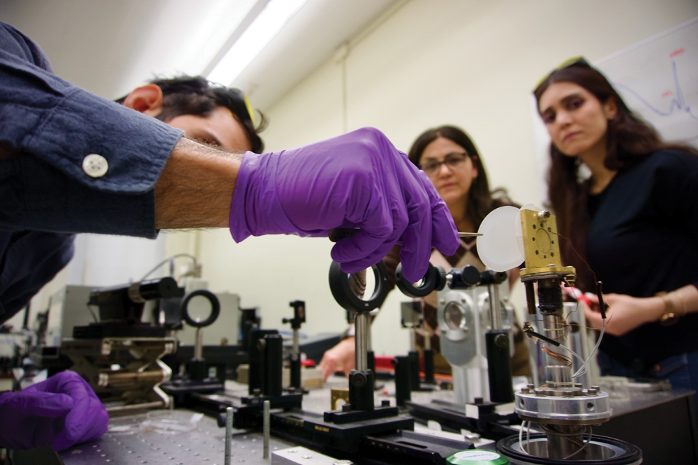
BY F. SHADI SHAHEDIPOUR-SANDVIK AND BENJAMIN MCEWEN FROM THE STATE UNIVERSITY OF NEW YORK-ALBANY AND DENIS DEMCHENKO AND MICHAEL RESHCHIKOV FROM VIRGINIA COMMONWEALTH UNIVERSITY
Sales of GaN-based semiconductor devices are on the up, driven by increased deployment in consumer electronics and integration within the automotive industry. According to market analyst Global Market Insights, revenue from GaN devices is forecast to climb at a compound annual growth rate of 6.8 percent until 2034, from over $22 billion in 2024.
Spurring this considerable success is the great set of properties of this wide bandgap semiconductor. GaN is renowned for its high-power efficiency, its excellent thermal management, and its support for miniaturisation.
Today, it’s hard to imagine a world without the first multi-billion-dollar GaN device, the LED. It’s certainly fair to say it would not be as bright. Without this game-changing emitter, many energy-efficient applications that humanity has been enjoying for nearly three decades would not have emerged at the same pace.
Underpinning all this progress is the work of Hiroshi Amano and his colleagues, who made a pivotal breakthrough in GaN technology, demonstrating that the p-type doping of GaN is possible. Realising this is a crucial step to the development of the LED, a class of p-n diode that put GaN on the map.

Figure 1. (a) Photoluminescence spectra from beryllium-doped GaN. (b)
Electron transitions to beryllium-related states. The polaronic states
of BeGa (Be1 and Be2) are responsible for the broad yellow luminescence (YLBe) band with a maximum at about 2.15 eV, whereas transitions via the BeGa
shallow state (Be3) can be observed only at temperatures above 100 K as
an ultraviolet luminescence band with the zero-phonon line at around
3.26 eV (labelled UVLBe3).
Despite the remarkable success of GaN technology from the 1990s onwards, p-type doping is still suboptimal. In most GaN-based devices, around just 1 percent of the magnesium acceptor dopant in the p-type layer produces free holes – that’s two orders of magnitude lower than the total magnesium concentration. In sharp contrast, acceptors in silicon exhibit nearly complete activation at room temperature.
Note that conductive p-type III-nitride materials are not just needed for LEDs. Realising p-type doping in the family of GaN materials, which includes AlN and AlGaN alloys, is essential for next-generation bright deep-ultraviolet LEDs (DUV LEDs), high-power electronic devices, and UV photodetectors.

Figure 2. Charge density of the hole localized on the neutral beryllium acceptor in GaN. (a) Deep polaronic state localized along Be-N bond in the c-direction of the wurtzite GaN (labeled Be2 in Figure 1); (b) in-plane deep polaronic state (labeled Be1 in Figure 1); (c) shallow state (labeled Be3 in Figure 1).
DUV LEDs are particularly promising for combating pandemics, disinfecting water sources, and sterilising surfaces. However, today’s commercial DUV LEDs emitting within the germicidal wavelength range, which spans 254 nm to 285 nm, have efficiencies below 5 percent and cost about 100 times more per watt than mercury vapour lamps. Meanwhile, in the wavelength range of 220 nm to 250 nm, the external quantum efficiency of DUV LEDs is even lower, below 1 percent.
A significant limitation in AlGaN-based devices, including those associated with DUV LED technology, is the absence of a low-resistivity p-type layer. While magnesium remains the only viable acceptor, its ionisation energy (EA) is relatively high. In GaN, it’s 0.22 eV, a value that increases with the bandgap of the III-nitride alloy, rising to 0.5-0.6 eV in AlN. Due to this, magnesium doping is inefficient.
To address this issue, some research teams have turned to alternative approaches, such as superlattice structures and polarisation-induced hole doping. However, there are downsides to these methodologies, including lower vertical conduction compared with lateral conduction. Due to these drawbacks, there is tremendous demand for uncovering a shallower acceptor in GaN, AlN, and AlGaN that offers a lower ionisation energy than magnesium.
A beryllium boost?
Offering one potential solution is the replacement of the magnesium acceptor with beryllium, which is routinely used as an acceptor dopant in other III-Vs, such as GaAs. This approach has much promise, given that theoretical and experimental evidence suggests that beryllium has a shallower acceptor level than magnesium in (Al)GaN.
Beryllium, a group II element directly above magnesium, is a divalent atom that’s a suitable acceptor dopant in III-V materials when it substitutes for group III elements. According to early density functional theory calculations in the late 1990s by Fabio Bernardini and co-workers from the University of Cagliari, Italy, the beryllium acceptor level is less than 100 meV above the GaN valence band maximum. Experimental evidence broadly confirmed these predictions. However, beryllium-doped GaN, often almost exclusively grown by MBE at relatively low temperatures, tends to exhibit semi-insulating behaviour.
Under a National Science Foundation grant, our team from the University of Albany and Virginia Commonwealth University has pioneered a systematic approach to growing beryllium-doped GaN using MOCVD, the most widely used growth system in the manufacture of III-nitride devices. Due to higher growth temperatures compared with MBE, MOCVD-grown GaN has dislocation densities that are generally about an order of magnitude lower, making this epitaxial technology an attractive choice for the development of novel doping methods.
With MOCVD, the biggest challenge is that the beryllium source cannot simply be metallic, as is the case in MBE. What’s more, due to the high toxicity of beryllium metal-organics, precursors for MOCVD are difficult to obtain, making beryllium implantation a potentially attractive doping process for those wanting to take advantage of MOCVD’s good material quality, high throughput, and scalability. However, ion implantation induces material damage and donor-defects, making it extremely difficult to obtain p-type III-nitrides without the use of in situ doping.
Breaking new ground, we have used beryllium acetylacetonate (Be(acac)2) as a beryllium precursor and developed MOCVD growth processes for in situ doping that maintain a high material quality and a relatively low compensation.
Note that we are enthused by recent work from Alan Doolittle’s team from Georgia Institute of Technology, involving beryllium doping of AlN via metal-modulated MBE. This team has demonstrated conductive p-type AlN, realising room-temperature hole concentrations and conductivity of up to 4.4 x 1018 cm-3 and 0.045 Ωcm, respectively.
We have undertaken extensive photoluminescence studies of our MOCVD-grown, beryllium-doped samples. We routinely observed the presence of the UVLBe band, indicating a beryllium-related shallow acceptor with an ionisation energy of 113 meV in our GaN. Initially, we mistakenly attributed this to the isolated BeGa acceptor. However, our subsequent photoluminescence studies have provided us with compelling evidence that BeGa is a dual-nature acceptor, featuring: two polaronic deep states, located at 0.38 ± 0.03 eV and 0.33 ± 0.05 eV above the valence band minimum; and a shallow state, with a delocalised hole at 0.24 ± 0.02 eV above the valence band minimum (see Figure 1).
Through photoluminescence studies of over fifty beryllium-doped GaN samples grown by MOCVD and MBE, we have demonstrated that the UVLBe band at 3.38 eV – the signature of a shallow beryllium-related acceptor in GaN – cannot be attributed to isolated BeGa. Nevertheless, the defect responsible for the 3.38 eV band clearly contains beryllium and exhibits features of the shallowest acceptor in GaN. This suggests that conductive p-type beryllium-doped GaN is feasible, if one can understand the nature of the shallowest acceptor (EA of 113 meV) in beryllium-doped GaN. Recently, using hybrid density functional calculations, we have proposed that this could be the BeGaONBeGa complex (see Figure 1). Figure 2 shows the charge densities of the hole localized on the two polaronic states (a, b) and the shallow state (c) in the crystal lattice of GaN, calculated using the hybrid density functional theory.
Another promising strategy for achieving conductive p-type GaN is co-doping. We expect that co-doping with beryllium and oxygen could lead to an abundance of BeGaONBeGa acceptors, with a concentration exceeding that of compensating donors. It’s possible that high concentrations of mobile gallium vacancies will facilitate the formation of the complexes during MOCVD growth in nitrogen-rich conditions.
There’s also a promise associated with strain-enhanced doping. For example, indium, often used as a surfactant, might induce compressive strain during growth, offsetting the tensile strain from beryllium incorporation. Due to the highly volatile nature of indium at common MOCVD GaN growth temperatures, typically more than 900 °C, little to no indium incorporates into GaN, making it an excellent surfactant that affects growth without incorporating into the material.
To unlock the full potential of III-nitride semiconductors, our community must overcome the persistent challenge of p-type doping. Ultra-wide bandgap materials, such as AlGaN, represent a particularly promising frontier, especially given their foundational ties to the advancements already made with GaN. However, magnesium-doping alone cannot produce p-type aluminium-rich AlGaN or AlN, due to the high acceptor depth of magnesium in these materials.
Our preliminary research suggests that beryllium, possibly in the form of impurity complexes, could hold the key to enabling high-efficiency, conductive p-type (Al)GaN. Theoretical studies and experimental evidence both point toward beryllium-related shallow acceptors as a critical component in this pursuit.
While p-type doping in GaN and its alloys remains a complex puzzle, it’s also an exciting opportunity. Advancing this field could catalyse a new wave of technological innovation, with applications ranging from next-generation displays to energy-efficient power electronics and life-saving DUV LEDs. If history has shown us anything, it’s that the brightest ideas often come from solving the toughest problems – and we’re optimistic that this challenge will be no exception.


