‘Smart stamp’ offers new way to transfer microLEDs
Scientists at Hong Kong University of Science and Technology have used an array of microscopic heaters and a phase-changing polymer to selectively pick up and place delicate electronic components, ranging from tiny microLEDs to nanometer-thick films. Similar programmable systems could be used to mass-produce defect-free displays and stack three-dimensional microchips, the researchers say.
Yunda Wang and his team have been investigating ways to sort and assemble microscopic devices for large-scale manufacturing. The current industry standard for transferring these components works like a giant rubber stamp, picking up entire arrays at once. This makes it difficult to selectively replace defective pixels during display manufacturing. Alternative methods use lasers to release specific chips, but they rely on expensive optical systems and risk damaging fragile materials with high heat.
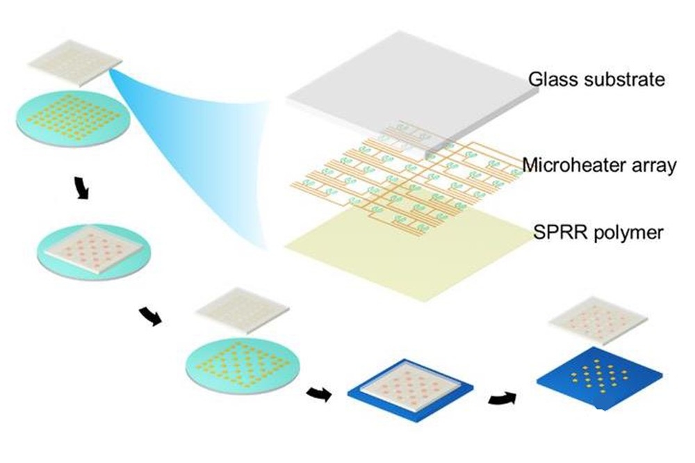
The team's latest work 'Microassembly of multi-material and 3D integration enabled by programmable and universal high-precision micro-transfer printing', published in the International Journal of Extreme Manufacturing, involved building a dynamically programmable transfer head that uses localised heating to control a polymer's stickiness.
The team successfully transferred semiconductor chips, 90nm-thick copper films, and perfectly spherical 50µm polystyrene beads. The components were placed with high precision, showing a positional drift of less than 0.7µm and a rotational error under 0.04 radians.
To build the system, Wang and his colleagues formulated a specific polymer that undergoes a sharp physical transition, changing from a rigid plastic to a rubbery state at exactly 44 °C. They coated a 30µm-thick layer of this polymer over an array of individually controllable microheaters.
During the transfer process, the stamp presses against an array of components. The team activates specific heaters, melting targeted 50µm spots of the polymer in about 60 milliseconds so it conforms to the selected chips. As the polymer naturally cools down in roughly 40 milliseconds, it hardens and physically locks onto the chips. To drop the components at their new destination, the heaters are triggered again, softening the polymer to release its grip. This temperature-driven mechanism provides a pickup-to-release adhesion strength ratio higher than 190 to 1.
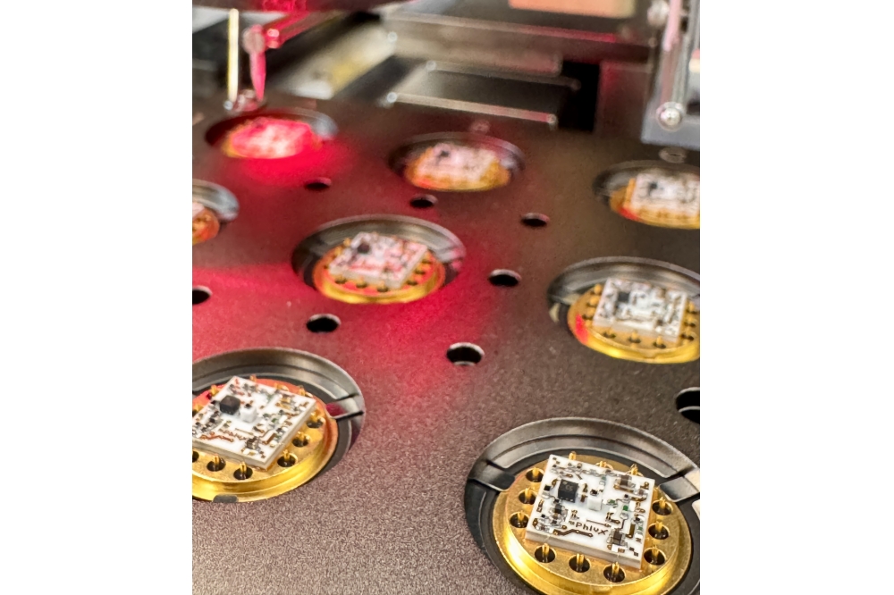
The team says the most promising applications for this selective transfer technology are in managing pixel yields for high-resolution microLED displays, where even a 0.01 percent defect rate can translate to thousands of dead pixels. The researchers proved their system could selectively sort and transfer functioning 45-by-25µm microLEDs to form custom layouts without degrading their performance.
They iare now investigating ways to scale up the microheater array. This poses a challenge because densely packed heaters can cause thermal crosstalk, where heat bleeds into adjacent pixels. To overcome this, the researchers plan to use thinner polymer layers and introduce active-matrix driving circuits — similar to the architecture used in commercial flat-screen televisions — to manage massive arrays without requiring overwhelmingly complex wiring.