
GaN-on-silicon HEMTs for tomorrow’s handsets?
A collaboration between A*STAR, Nanyang Technological University and Soitec is claiming to have broken new ground in the development of GaN-on-silicon HEMTs for wireless communication. The team’s transistors combine two critical attributes for transmit/receive modules, namely high efficiency and low noise, despite a level of scaling that’s described as moderate (the gate length is 100 nm).
Due to these strengths, the GaN HEMT is a compelling candidate for replacing the GaAs HBT, the dominant semiconductor technology in RF front-end modules in cell phones for more than a decade. It is forecast that wireless communication will move to higher date rates, which require higher bandwidths at higher frequency ranges, a non-negiotiable that plays into the hands of the wider bandgap transistor technology.
According to team spokesman Qingyn Xie from A*STAR’s National Semiconductor Translation and Innovation Centre for Gallium Nitride, another asset of the GaN-on-silicon HEMT over the HBT is its higher power density, a valued characteristic in the power amplifier (PA). “With backward compatibility concerns, the same chip area must support a wide range of bands, therefore power density becomes a critical parameter,” argues Xie.
According to the A*STAR researcher, another advantage of the GaN-on-silicon HEMT is its higher breakdown voltage, which promises to enable a more robust technology that could simplify on-chip protection circuits. And as GaN-on-silicon HEMTs could be manufactured using 300 mm CMOS-compatible GaN-on-silicon processes, these transistors could fulfil demand for mass-market, low-cost components.
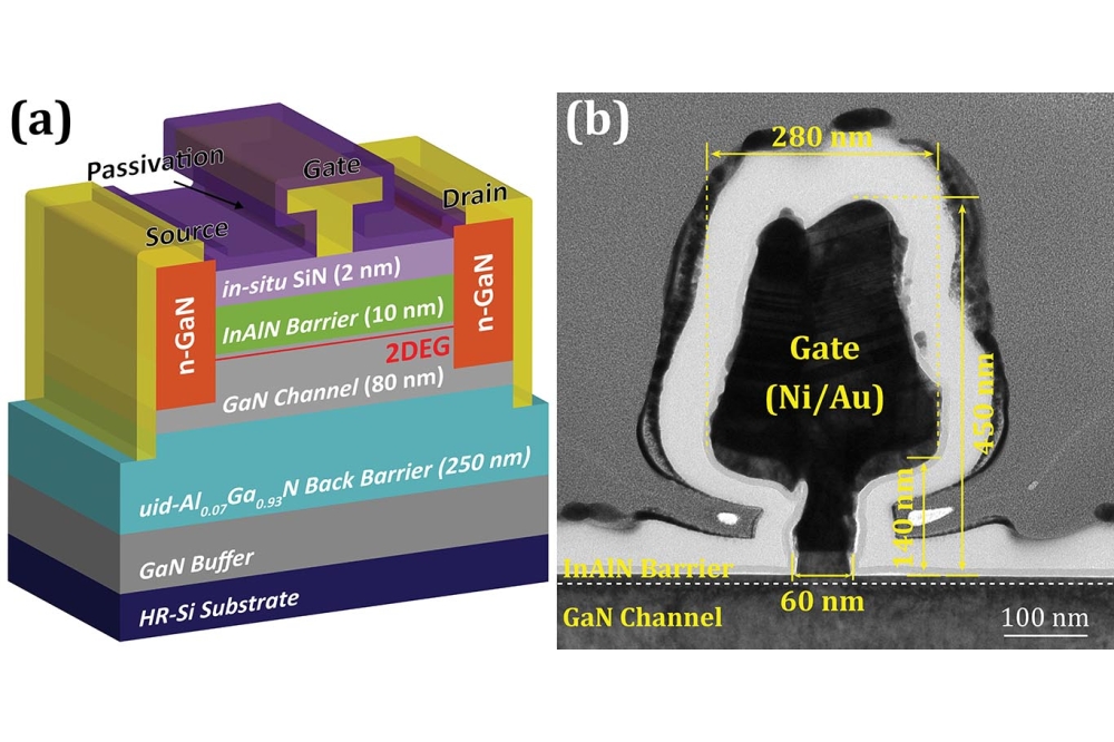
Production of the transistors involved processing MOCVD-grown 150 mm epiwafers featuring high-resistivity silicon substrates. The heterostructure has a carbon-doped GaN buffer optimised for RF performance, a 250 nm-thick unintentionally-doped Al0.05Ga0.95N back barrier, an 80 nm-thick channel, a 10 nm-thick InAlN barrier and a 2 nm-thick SiN cap.
The InAlN barrier provides strong polarisation and a low gate-to-channel distance, enabling improved two-dimensional electron gas control; and the ultra-thin GaN channel and AlGaN back-barrier enhance electron confinement, effectively supressing short-channel effects and lowering channel noise.
Fabrication of the HEMTs involved etching, lithography, MBE re-growth of n-type GaN, the formation of T-shaped gates, atomic layer deposition of Al2O3, and plasma-enhanced CVD of SiN. Using these steps, the team produced HEMTs with a source-to-drain spacing of 2 mm, a gate width of 2 x 25 mm, and gate lengths of 60 nm, 100 nm and 150 nm.
Characterisation of these devices determined a maximum drain current of 1.58 A mm-1, an on-resistance of 1.48 W mm, and a threshold voltage of -2.9 V. Operating under a drain-source voltage of 10 V, the cut-off frequency and maximum oscillation frequency are 100 GHz and 254 GHz, respectively, for the HEMT with a 100 nm gate length. Under continuous-wave operation at a gate-source bias of -2.8 V, the HEMT with a 100 nm gate length produces a saturated output power density of 1.19 W mm-1, a power-added efficiency of 62.3 percent, and a linear gain of 11.1 dB.
The team have also evaluated low-noise performance, described as ‘outstanding’. Across 10 GHz to 40 GHz, the minimum noise figure is less than 1.4 dB, suggesting that this HEMT could be deployed as a low-noise amplifier (LNA) in next-generation smartphones.
“In the future, if the RF switch performance using this GaN-on-silicon process would be promising, this GaN-on-silicon process could theoretically be used for the LNA, PA, and switch, therefore forming a monolithically integrated transmit/receive module,” says Xie. “Such on-chip solutions are desired for millimetre-wave communication, due to the lower parasitics.”
One of the plans for the team is to optimise these devices for higher performance at low voltage, which may be accomplished by trimming the on-resistance, via shrinking the source-drain distance while maintaining the gate length and other process features. “Secondly, we will explore E-mode transistors; and thirdly, we hope to characterise the linearity of these transistors,” added Xie.
Pictured above: The GaN-on-silicon HEMT technology targeting millimetre-wave applications features a T-shaped gate and bilayer passivation.
Reference
Y. Zhuang et al. IEEE Electron. Dev. Lett. 47 482 (2026)


