
k-Space supports next generation of materials science students
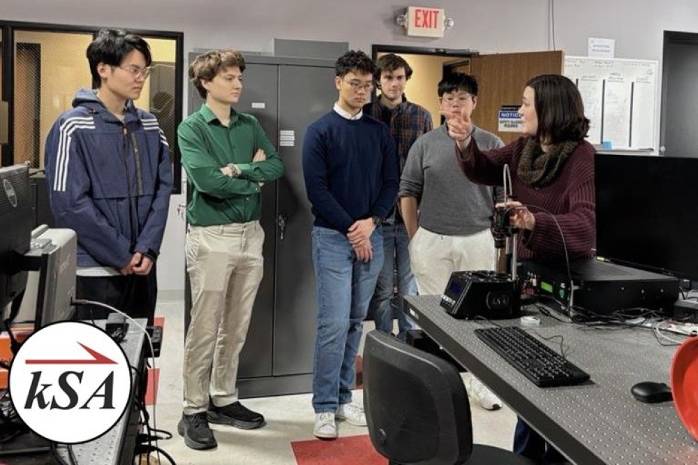
Earlier this year, students from the University of Michigan Materials Science & Engineering (MSE) program visited the firm k-Space to learn about thin-film metrology and to receive training on the kSA BandiT, which was essential for their project, 'Seeing Through Thin Films: A Model for Accurate Band-Edge Thermometry.'
The team took on a practical challenge: because BandiT calibration curves depend on substrate thickness — and a single curve takes about nine hours to generate — they set out to develop a faster way to account for small deviations in substrate thickness, without running a full calibration each time.
k-Space’s Brenna Yorimoto, PhD, first introduced students to kSA 400 and kSA BandiT, before providing guidance on their experiment. Once trained on the kSA BandiT, the students got to work. As they noted, band-edge thermometry is a high-precision, non-invasive way to measure the in-situ temperature of semiconductor thin films in vacuum. It takes advantage of the linear relationship between bandgap and temperature, which is the basis of the kSA BandiT.
Over several visits to the k-Space engineering lab, the students built a mathematical model to interpolate between thicknesses, refined it, and evaluated the results. Each calibration curve used to train the model was generated using the following process; Selected samples of varying thickness that were otherwise similar, Cut samples and load into a vacuum chamber, heat the sample to maximum temperature under vacuum, capture band-edge spectra with the kSA BandiT while cooling, and process the raw data.
The students explored two approaches: a polynomial-fitted-coefficient model and a linear-plus-Gaussian fit of the raw data. Both achieved strong predictive performance (R² of 0.993 and 0.986, respectively), validating the underlying approach.
The team summarised their work in the poster here. They hope the project can be continued — with students collecting more data to improve accuracy (their initial sample size was small due to time constraints), incorporating dopant concentration as a model parameter, and extending the approach to materials beyond silicon, such as GaAs and InP.


