

Yole predicts a bright future for InP
Latest report forecasts $172 million market by 2024
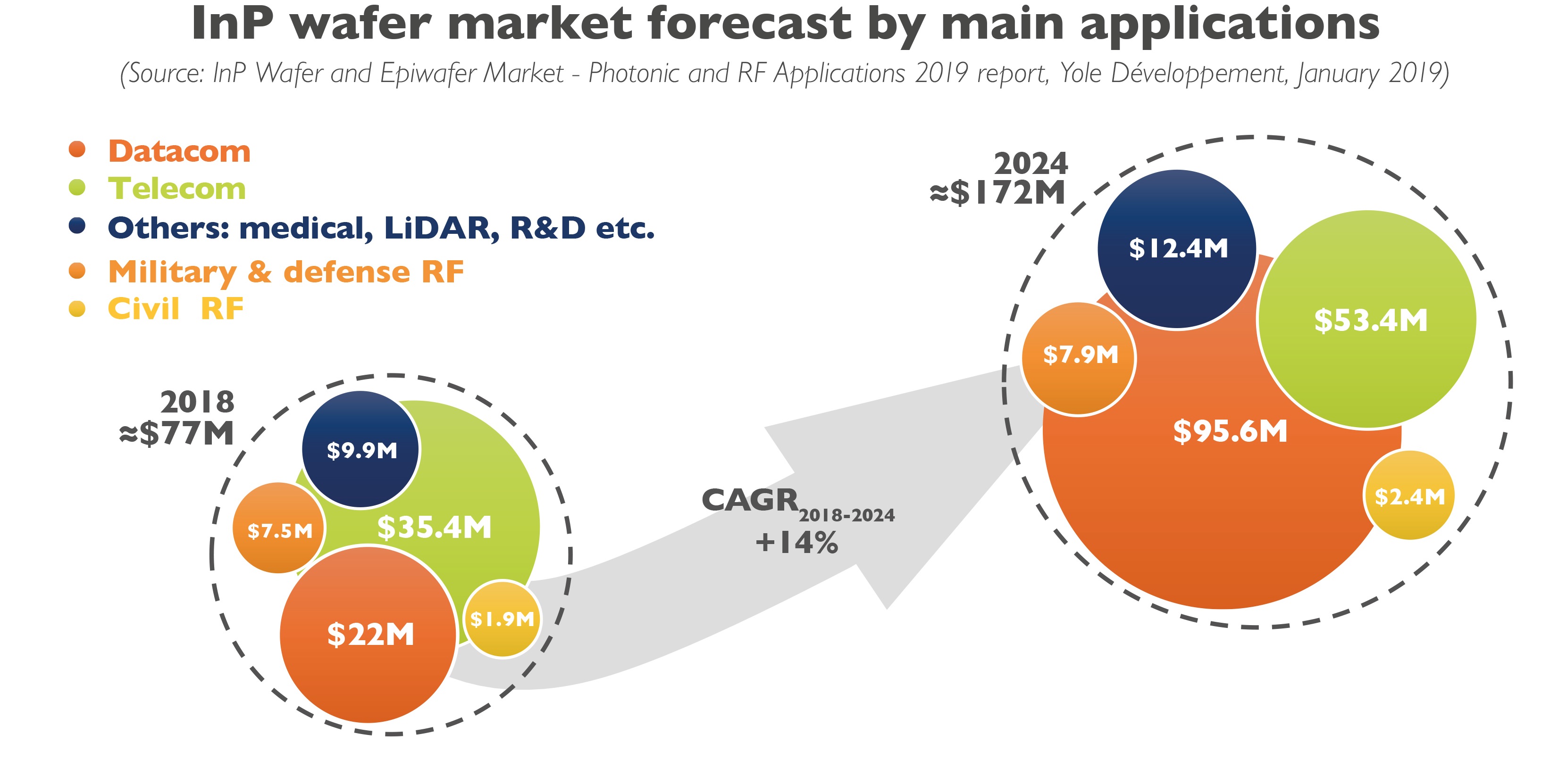
As an old but gold-standard member of the compound semiconductor family, InP possesses the key advantages of emission and detection capabilities over 1000nm in the photonics domain, as well as high speed and low noise performance in high-frequency RF applications. Now, driven by the arrival of 5G and the impressive growth of datacom business, the InP wafer and epiwafer are doing very well. Yole Développement in its latest report forecasts a $172 million market by 2024, with a 14 percent CAGR between 2018 and 2024.

The InP wafer market is today dominated by the high-speed fibre optic communication market, as InP is capable of emission and detection in wavelengths above 1000nm. The InP wafer market is so largely impacted by the photonics market, especially driven by datacom and telecom applications: each market segment is using InP as a substrate for both laser diodes and photo diodes in optical transceivers.
Currently, the main boost for the InP wafer market is expected in photonic applications. In optical communication, InP offers high performance in many functions including emission, photo detection, modulation, and mixing, but it is often challenged by other semiconductor platforms because of its high cost. Nevertheless, InP is an indispensable building block for laser diodes in transceivers used for telecom and datacom applications. Specific to the cyclic telecom market, which has recently slowed down, massive investment plans from different operators (i.e. China Telecom) are expected with the imminent 5G network.
“In fact, the InP wafer market for telecom is projected to reach around $53 million by 2024,” comments Hong Lin, senior technology and market analyst at Yole. Also, significant investment in the datacom market is expected from different players, led by internet giants Google, Amazon, Alibaba, and more.
With the requirement of more data transfer at higher speeds, transceiver technology is migrating to technology offering better rates (100GbE and 400GbE), for which InP is more favourable. The wafer market for datacom is expected to explode, with an impressive 14 percent CAGR between 2018 and 2024. Last but not least, exciting LiDAR applications could be promising for InP, i.e. enabling eye safety at higher wavelength, which is currently in an early R&D phase.
Yole is deeply involved in the compound semiconductor sector, covering SiC, GaN , GaAs and InP. This week, the company is organising an online event dedicated to the GaAs industry. Sponsored by IQE, the 'GaAs Wafer and Epiwafer Market: RF, Photonics, LED, and PV Applications' webcast takes place on January 30 at 5.00 PM CET – 8.00 AM PDF. Ezgi Dogmus from Yole and Drew Nelson president & CEO of IQE, will present the status of this industry and point out the technology challenges.
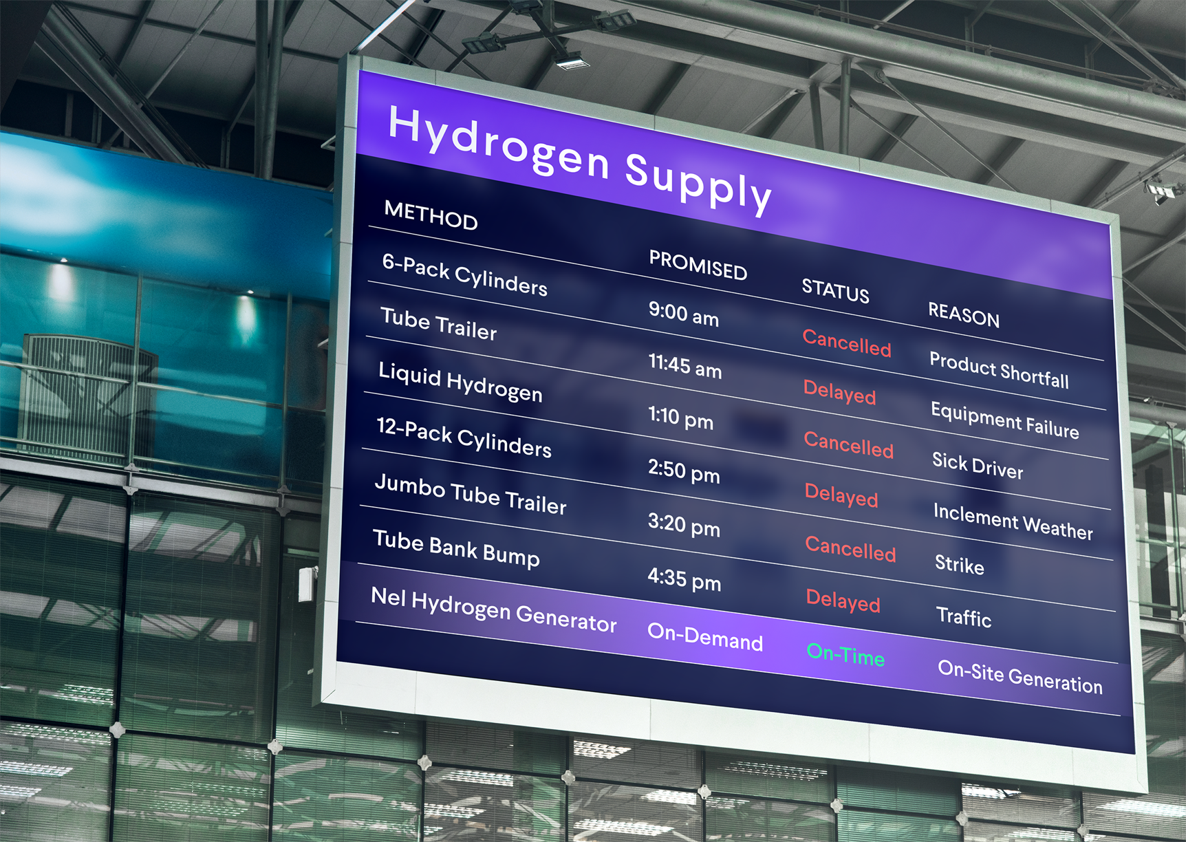
Secure Your Hydrogen Supply
A study supply of high-purity hydrogen is critical to semiconductor fabrication. Supply chain interruptions are challenging manufacturers, leading to production slowdowns and stoppages. On-site hydrogen generation offers a scalable alternative for new and existing fabs, freeing the operator from dependence on delivered gas.Plant managers understand the critical role that hydrogen plays in semiconductor fabrication. That important job includes crystal growth, carrier gas, wafer annealing, and in the emerging Extreme UV Lithography (EUV) that will enable new generations of devices. As the vast need for semiconductors grows across all sectors of world economies, so does the need for high-purity hydrogen.
Take control with Nel on-site hydrogen generation.
Read more