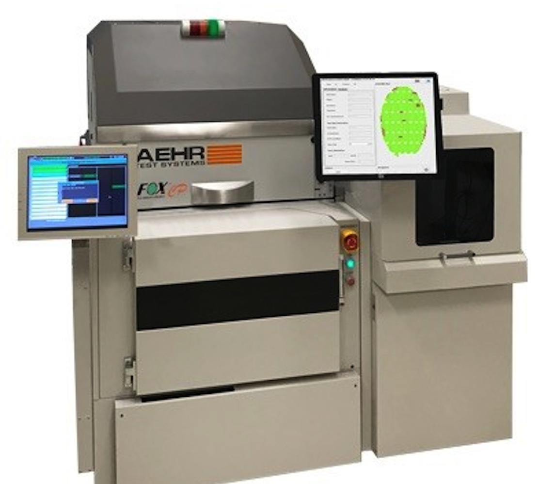
Aehr Wafer Test system targets photonics

FOX-CP system features unique capabilities for testing and reliability screening of VCSEL arrays
Aehr Test Systems, a Fremont-based supplier of semiconductor test and burn-in equipment, has introduced the FOX-CP system, its new low-cost single-wafer compact test and reliability verification solution for logic, memory and photonic devices such as VCSELs.
Aehr will show the new system at the SPIE Photonics West conference being held at the Moscone Convention Center in San Francisco February 5-7, 2019.
Gayn Erickson, president and CEO of Aehr Test Systems, commented: “The new single-wafer FOX-CP system is integrated with a wafer prober and performs wafer-level testing and reliability cycling for logic, memory and photonic devices. This newest addition to our FOX-P product family is optimal for test times ranging from minutes to a few hours or where multiple touchdowns are required to test the entire wafer. It complements the capabilities of the FOX-XPTM and FOX-NPTM systems, which are optimal when the test time is measured in hours or days and the full wafer can be tested in a single touchdown. The FOX-CP system offers a low-cost integrated package for both initial evaluations and production applications."
“We are very optimistic about the silicon photonics and photonics sensors markets and believe they will be significant growth drivers for Aehr. The rapid growth of integrated optical devices in high-performance servers and data centers, mobile devices, automotive applications, and now wearable biosensors is driving substantially higher requirements for initial quality and long-term reliability, and the requirements are increasing with every new product generation. We believe these new applications are driving an entirely new level of quality and reliability expectation for these systems and pose a significant long-term growth opportunity for Aehr.”
Photonics Applications
The FOX-CP system features unique capabilities for testing and reliability screening of VCSEL arrays for 3D sensing applications and silicon photonics for 5G communications application. These include:
Testing tens of thousands of arrays per wafer with amps of current per array.
Stabilising lase and identifying infant mortalities through extended stress/test programs.
Electrical and go/no-go optical detection.
One application is to conduct single touchdown sampling test to confirm the processing of the wafer is within specified limits and the yield exceeds minimum requirements. The large number of 2A channels (4A with pulsing) available enables a large sample size (as many as 1024 die) with a single touchdown, while providing an individual power supply per die. Individual power supplies per die enable maximum monitoring for device reliability characterisation.
Another application is to perform multiple touchdown (stepping) aging of the full wafer to stabilize the lasing parameters of the die. The large number of high-current power channels can reduce the number of steps by an order of magnitude and increases production throughput. Stabilizing/aging the lasers allows higher-bandwidth performance of the end product, since the laser parameters can be matched and don’t change over time and brings the laser parameters into the narrow range required for effective control of the devices.
FOX-P Platform
According to AEHR, features of the FOX-P platform that contribute to its cost-effectiveness include the ability to provide up to 2,048 'Universal Channels' per wafer or DiePak carrier, which allows the system to test all the devices on the wafer or DiePak carrier in parallel. The Universal Channel architecture allows any channel to be any function (I/O, Device Power Supply (DPS) or Per-pin Precision Measurement Unit (PPMU)). This allows customers to do per pin parametric testing, more extensive digital pattern test with deeper data stimulus / capture memory (32M per pin), and deeper scan (768M) optimised for BIST/DFT testing.


