

Minimizing implant-induced damage in GaAs ICs
Introducing an electron-shower current in an ion-implanter eliminates charge-induced damage in GaAs epiwafers
BY LAM LUU-HENDERSON, SHIBAN TIKU, MEHRAN JANANI, JOHN BONK, STEVE CANALE AND MARK BOREK FROM SKYWORKS SOLUTIONS
One of the most complex, persistent sources of yield loss in the IC industry is damage caused by electrical discharge.
Given that the silicon industry has a greater level of maturity than that of our own, it is no surprise that there is a considerable history and established methodology for addressing charging effects in silicon IC manufacturing. In those fabs, there is a potential for yield loss during the ion implantation step, commonly used to produce active devices. For certain processes, this step is carried out after the deposition of a dielectric layer, such as a gate oxide.
In addition, there may be charge-related yield loss in silicon fabs, due to the exposure of wafers to plasma treatment. During this step, which follows the formation of transistors or capacitors, damage to active and passive devices can occur due to electrical discharge accumulated during various ion bombardments.
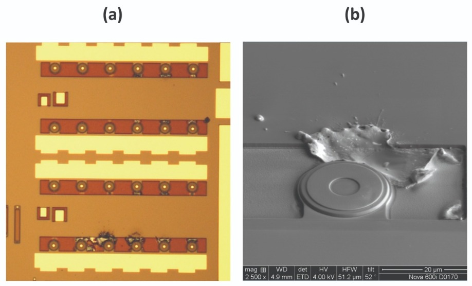
Figure 1. (a) Electrical charging defects on a pilot lot for a Skyworks HBT transistor array (b) Scanning electron microscopy image of the charging damage to the HBT structure
For those that work in the III-V industry, there is far less literature to draw on that are related to electrical discharge damage – and experience associated with this yield-loss mechanism is more limited. So, to address this weakness, our engineering team at Skyworks Solutions, a manufacturer of GaAs HEMT and HBT products, has undertaken an extensive study and analysis of this phenomena. Drawing on expert guidance from Axcelis Technologies and Innovion Corporation, we have explored yield impact, failure mechanisms and possible solutions associated with implant-induced charging failure.When processing III-Vs, a potential source of electrically induced defects is the plasma system, because it generates a high voltage on the wafer. To prevent generation of reliability impacting imperfections, proper precautions are needed to protect the wafer.
A noteworthy difference between the silicon IC industry and that of our own is that we do not employ an oxide or insulator under the gate. Consequently, electrical discharge avoidance is not common practice. In our industry, it is rare to produce ion implanted active layers – dopants tend to be introduced during the growth of epilayers. That’s not to say that ion implantation has no role to play; it is used to isolate regions of a wafer. This is normally undertaken with medium-current ion implanters, but the beam current can still exceed the limit for producing electrical damage.
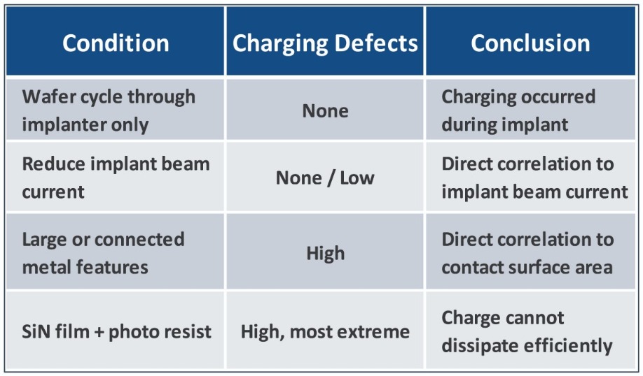
Table 1. Summary of critical experimental results to determine the origin of charging defects in HBT arrays.
Working with heliumDevice isolation in our industry is normally accomplished with the implantation of He++ or He+ ions. Due to the inherent nature of ion implantation, it is inevitable that charge build-up takes place on the wafer, despite some neutralisation of the helium beam as it traverses from its source to the target. The insulating photo resist layer and the semi-insulating nature of GaAs prevent the net positive charge, which can build up instantaneously, from adequately dissipating. This charge is an issue, as it can lead to extreme instances of electrical discharge failure.
Unfortunately, it is challenging to eliminate this charging effect on the devices on the wafer. This is particularly problematic when there are sufficient numbers of metal contacts on the wafer surface prior to ion implantation – charges can accumulate at these contacts and go beyond the threshold for electrical damage. Note that the discharge current can be so high that it can cause melting and destruction of device structures.
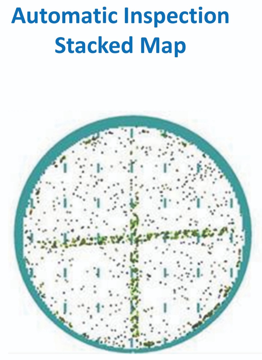
Figure 2. Stacked automatic inspection maps of damaged die, exposing a cross-hair and outer ring pattern with electrical discharge failures.
We reduce the chances of this yield hit by undertaking the isolation implant process early in the processing flow, because at this point the surface of the wafers has either none or very few metal contacts. If metal contacts are necessary prior to implant, we take action to minimize severe arcing-related damage, such as the reordering of the process steps. That’s not unusual: for technological advancement, at times process modules are reordered in the manufacturing flow to improve device performance, trim costs or increase the overall process efficiency.Pilot challenges
Several steps have been re-arranged during the development of our latest HBT process. During our evaluation of pilot lots, we observed several defects caused by severe electrical charging damage (see Figure 1). These charging-induced, blown-out defects contributed to visual and probe failures, and accounted for an overall yield loss of about 0.5 percent. Our inline automatic optical inspection tool uncovered visual defects, while functional leakage failure exposed the probe yield loss.
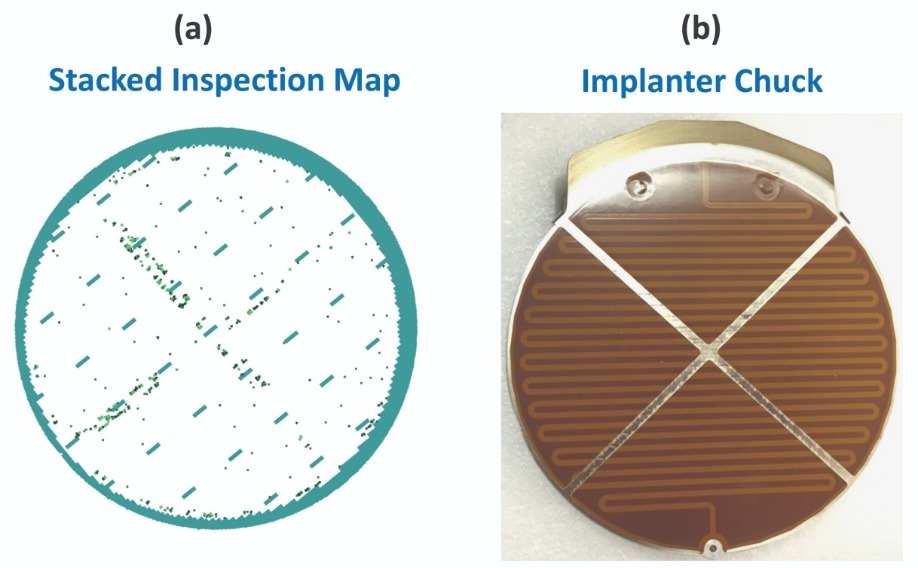
Figure 3. (a) The yield map of damaged die reveals a cross-hair pattern of electrical charging failures (b) In the Axcelis 8250 ion implanter, the electrostatic chuck ground path is in a cross and ring pattern, with the grounding pin to the left of the chuck.
To investigate the source of this extreme charging failure, we carried out a sequence of experiments, evaluating different types of epitaxial materials, photoresists, resist thicknesses and nitride film densities. Most of these variables had minimal impact on the failure rate. However, this study did uncover several strong correlations between the extent of the damage and key processes and tooling parameters, and ultimately it provided valuable insights into the mechanism of this failure.Our findings, summarized in Table 1, include our observation that our wafers do not exhibit any electrical discharge damage when they are cycled through the implanter without receiving any ion implant processing. That implies that the charges generated for these defects occur during the implant process, rather than from a build-up of charge on the implanter wafer station. We also found that the higher the implant beam current, the greater the severity of charging damage; and that failures appear to be highly area dependent, impacting the larger metal features far more than smaller, isolated ones.
Another observation is that when the wafers are covered by a nitride film or photo resist, they have the most severe charging defects. Particularly susceptible to this ailment are wafers with a blanket, unpatterned sheet of photo resist. This insight reveals that it is not possible to dissipate the charges that are accumulated during the implant process, due to the combined insulating effects of the dielectric, polymer and semi-insulating GaAs substrate.
Initially, we thought that our blown and melted features, which we discovered by inline visual inspection, were distributed in a fairly random manner across the wafers. But when we stacked up the inspection yield maps, we found a very distinct cross and outer ring pattern (see Figure 2).
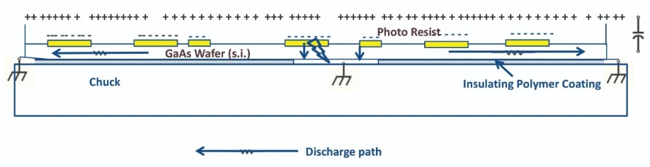
Figure 4. An illustration of the charge distribution across the wafer during implantation and the dissipation path through the grounded channels of the electrostatic chuck.
To uncover the cause of this pattern, we focused on the steps before and around the isolation ion-implantation. By carefully segmenting each process step and associated tool set, we determined that ion implantation is the source of the defect. The ‘smoking gun’ is a damage pattern that resembles the features of the cross and outer ring of our implanter wafer station, which uses an electrostatic chuck (see Figure 3).The implanter that we use is the Axcelis NV8250. The wafer station in our Axcelis NV8250 has been uniquely designed for GaAs processing, with the chuck divided into four equal quadrants so that the polarity of each of these sections can be reversed, enabling a better release of the wafer after it has been implanted. Note that the electrostatic chuck of this implanter is a modification to the original chuck offered by Axcelis. It is designed to tackle the frequent wafer breakage we faced with the original, single-outer-ring electrostatic chuck design. Prior to modification, we struggled to separate the wafer from the chuck after the implant step, due to excessive build-up of charge, which would not dissipate quickly enough to allow easy release of the wafer.
With the new chuck design, four sections are laid out in a cross configuration within the outer edge ring. With this arrangement, the entire surface of the chuck is coated with polymer, except for the aluminium cross-hair and the outer-edge ring areas – these are the only locations directly connected to ground through a grounding pin (see Figure 3(b)).
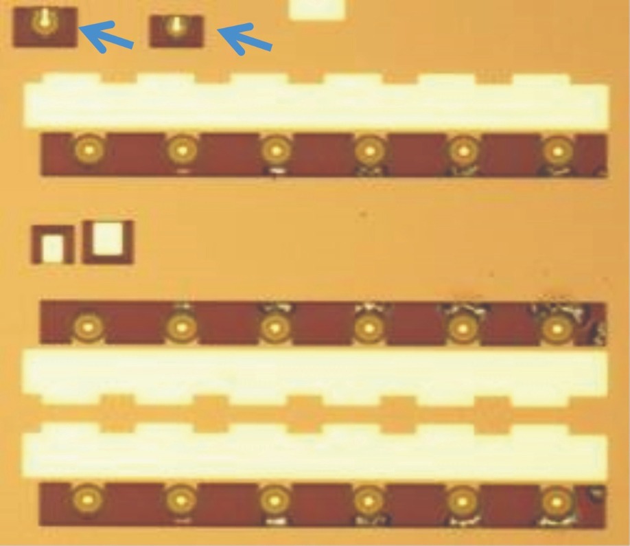
Figure 5. Electrical discharge induces damage on HBT transistor array, but the lone transistors are defect-free.
During implant, the wafer is in constant contact with the grounding pin. This ensures a proper dissipation of the net charge accrued on the metal contacts and on the wafer. However, with the new process flow, metal features are present. These are covered by SiN and the photoresist, both of which are insulators.Encapsulating the metal contacts with the nitride and photoresist films prevents the accumulated charge from dissipating. Although these contacts have a lower resistance than the epitaxial layers of the HBT, the epiwafer itself is semi-insulating; consequently, the least resistive path for the release of this charge build-up is through the grounded cross and outer ring of the chuck. Due to this, the concentration of the discharge current on the wafer metal features increases along the cross pattern and outer ring areas, leading to a higher probability for electrical discharge damage in those regions.
If they are exposed, the metal features on the wafer act as antennae; and if they are covered by photoresist, they charge up like capacitors – depending on position, size and shape – until the voltage builds to a critical level, followed by a fast discharge to ground (see Figure 4 for an illustration of this failure mechanism). Note that the path of resistance depends on the position on the chuck, and is lowest in the cross and ring.
As the beam current is cranked up, there is an increase in charge accumulation on the wafer. This results in current crowding around the grounding regions during implant, and subsequently increases the number of higher electrical-discharge failures. As expected, there is a direct correlation between the magnitude of the beam current and the extent of the charging damage.
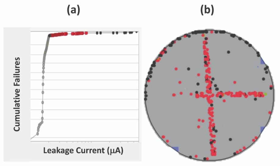
Figure 6 (a) Example of a leakage test detecting electrostatic damage failures. (b) A yield map showing failed dies in a cross and ring pattern.
Our explanation for the cause of wafer damage is consistent with the finding that the frequency of failures depends on the surface area. When metal contacts are larger, they will attract and accrue more charges, leading to even greater arcing effects. This is evident in optical images, where the smaller, isolated transistors are unaffected, while larger arrays of HBTs are more prone to the effects of electrical discharge (see Figure 5).Note that with product wafers, it is most common for the metal features to be under photoresist, and the remaining open field areas to be covered and implanted. However, in extreme cases, the whole wafer can be covered by photoresist, causing an aggressive build-up of charge, followed by catastrophic electrical charging failures.
To effectively identify these discharge failures, we have employed two modes of detection: automatic optical inspection, first after the implant step and again at the final outgoing die inspection; and a leakage probe test. The latter employs tighter limits to catch electrically weakened die that threaten to go undetected by automatic optical inspection and could potentially result in escapes. To identify these marginal and leaky die, we increased the bias voltage (see Figure 6 for the results of this approach).
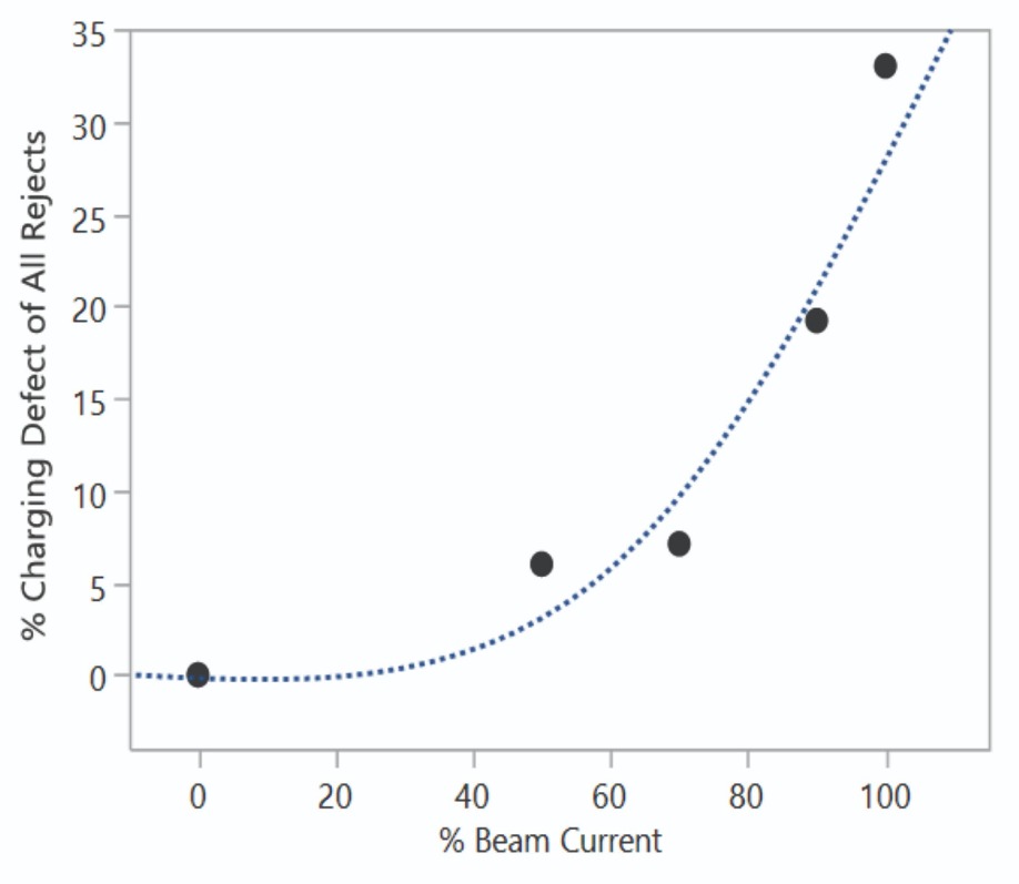
Figure 7. Charging induced defects increase as the implanter beam current rises.
Production solutionsWe live in an era of lean manufacturing, where it is often unfeasible to modify hardware for defects occurring at a level of parts per million. In these circumstances, alternative approaches are required to mitigate and contain these types of yield loss. One option is to dial back the implant beam current to limit the rate at which the ions hit the wafer. Ultimately, this decreases the charge collected at the contact metal, and should diminish the level of damage (see Figure 7).
To put this theory to the test, we varied the implant beam current from 0 percent to 100 percent, before immediately scrutinising implanted wafers with automatic optical inspection. After comparing the number of charging-induced failures with the total for detected defects, we observed a strong correlation between the beam current and the amount of charging damage.
Back in the 1980s, Eaton Corporation thoroughly studied and documented the role played by the implant current on the degree of charging on the wafer. They drew the same conclusion: reducing the implant current offers a quick, simple containment method for reducing the number of charging-induced failures. However, this undoubtedly comes at the expense of reductions in throughput and overall efficiency.
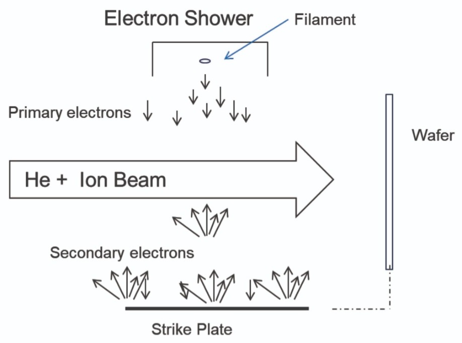
Figure 8. Charge-induced defects fall with the introduction of an electron shower into the end station, which features a single filament configuration. The strike plate is made of graphite to avoid contamination to GaAs circuits.
InAir transfer robot for the Axcelis NV8250.Source: Axcelis Technologies
Operator Interface and Load Station for the Axcelis 8250.Source: Axcelis Technologies
Another option for reducing charging-induced failures is to redesign the device structures to minimise electrical discharge damage. This approach, which may be challenging, involves implementing design-for-manufacturability rules that reduce the overall metal area. Charging and electro-static discharge failures are eliminated, by preventing any potential build-up of charge.This concept will be familiar to anyone that’s aware of the ‘antenna’ rules applied to the processing of silicon ICs. The basic principle is that the area of the wafer covered by a resist should not exceed a certain threshold. However, this can be hard to accomplish when undertaking isolation of some circuits, such as the HBT power array. In this case, the entire array can be 100 microns or more in length, but covered by a photoresist as a single entity, since electrically it is just a single device.
One way to comply with these rules is to configure the transistor collector contacts in the array so that they are just segmented electrically (see Figure 5). This ensures that each contact has a smaller conducting surface. Joining the contact areas together with an interconnect metal, deposited after the ion–implant step, trims charge build-up and reduces the likelihood of arcing-related events.
Showering with electrons
Out of all the options for addressing implant-generated charging defects, the most dependable and recommended is the industry-tested electron shower. Originally developed by Eaton Corporation, it has been widely adopted in the silicon industry.
In the case of our Axcelis NV8250 ion implanter, the electron-shower is integrated into the end station, where the wafer is staged for implantation. Using this design, electrons from the emitting filament flood the ion beam with a surge of negative charge, neutralizing positive He+ and He++ ions prior to implantation (see Figure 8).
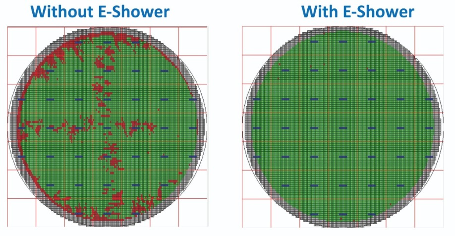
Figure 9. Yield maps of wafers with and without electron-shower during isolation implant.
With our tool, the electrostatic chuck holds the wafer horizontally prior to implant. However, once the ion beam is optimized for implantation, this chuck end-station moves to an upright position. As primary electrons hit the strike plate, secondary electrons are generated, ensuring that positive charge has no chance of building up. In addition, secondary electrons are generated when the beam hits the wafer surface (see Figure 8).Many high-volume, high-density IC fabs use tools with electron showers. It is a dependable technology, but there are risks, as there is the possibility of having charging defects from a negative potential. So, to avoid inducing discharge damage created from an overdose of negative charges, careful process development is essential when optimizing electron-shower settings. Engineers must tread a fine line between ensuring neutralization and preventing excessive negative charges.
To determine the optimal electron-shower settings, we performed a ‘design of experiments’. This involved GaAs wafers deposited with contact metal and coated with SiN, and also wafers with an unpatterned isolation photoresist, which provides an extreme condition for assessing the degree of charging damage. Both types of wafer were implanted with and without an electron-shower beam. Experiments revealed that wafers processed with an electron-shower were free from charging symptoms, while those without an electron shower exhibited a severe case of discharge damage (see Figure 9).
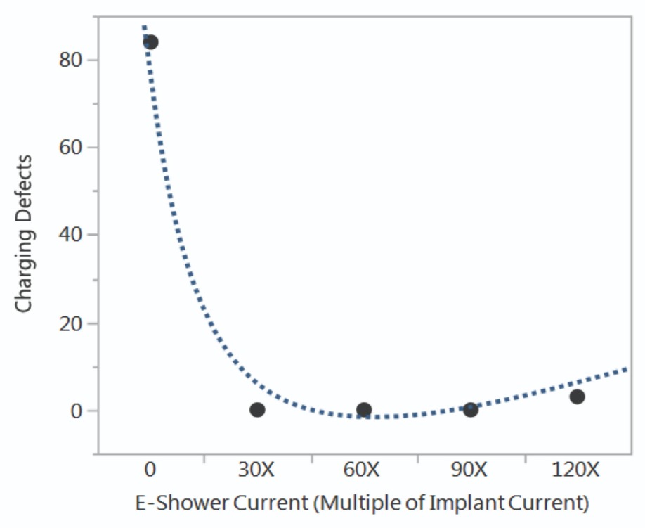
Figure 10. The charging-induced defect percentage as a function of electron-shower primary beam current, for a given implant recipe.
Note that there is flexibility with the medium-current implanter that we use. We could employ up to three filaments, but the recommendation is to use just one or two, so long as this provides sufficient neutralization. For our evaluation, we have used a single filament.It is recommended that the electron-shower primary current should be around thirty times the implant beam current. We have put this figure to the test, finding that even when the current is increased well beyond this recommended value, there is still zero to negligible implant charging-induced defects (see Figure 10). In other words, there is a very broad process window for using the Axcelis NV8250, while realizing an extremely low probability of negative charging.
By undertaking several iterations of our design-of-experiment, we have determined the ideal electron-shower process conditions for the Axcelis NV8250 implanter. In turn, this has led to improvements in optimal isolation and cycle times, as well as a major improvement to the electrical charging yield loss.
Our work shows that electrical charging and its consequent damages are not limited to the silicon IC industry, but extend to the makers of ICs based on
III-Vs. Charging can occur in all process steps involving plasma or charge beams. In particular, failures can be traced back to the ion implantation step used during the isolation process, which has the potential to produce heavy, visible damage to metal features. If the order of processing is changed, or there is a modification to process steps that involve charge species, there is the threat that this new routine creates visible or optically undetectable defects.
In our case, our new process flow has involved covering semi-insulating wafers, which have existing metal features, with insulating SiN and photoresist, prior to an ion-implantation step. Unfortunately, this combination creates the ideal condition for a catastrophic electrical discharge yield event. To get to the bottom of this issue, and ultimately determine the best way forward, we undertook a detailed assessment of these implant induced failures, followed by thorough experimental analysis. The discoveries that followed have enabled us to uncover the primary failure mechanism, and unlocked the door to critical preventive methods, proper quality control measures and overall improvement to product yield and reliability.


