
Making microLEDs on metal foils
The manufacture of microLED displays can take a big step forward by switching to the monolithic integration of transistors and LEDs grown on metal foils
BY VLADIMIR MATIAS AND JULIAN OSINSKI FROM IBEAM MATERIALS
Every year, billions and billions of LEDs are made by growing epitaxial layers of GaN and its related alloys on sapphire and silicon substrates. But that’s not the only option. At iBeam Materials of Santa Fe, NM, we have recently demonstrated that high-quality epitaxial GaN can also be deposited on polycrystalline flexible metal foils. Our technology opens the door to large area, lower-cost production of GaN-based devices with a process that is amenable to roll-to-roll manufacturing.
The approach that we employ involves ion-beam-assisted deposition. It is used to deposit a single-crystal-like intermediary layer, which forms the foundation for subsequent epitaxy of nitride layers. Working in partnership with researchers at Sandia National Laboratories and the University of New Mexico, we have used this technology to demonstrate practical LEDs through a project funded by the US Department of Energy, APRA-E (see Figure 1).
One of the more attractive opportunities for our ground-breaking technology is in microLED displays, which require large areas of low-cost LED arrays. The most common approach to making these arrays is based on singulation and mechanical transfer. However, there is a move to ever smaller LEDs, making this technique more challenging to implement. It is far better to adopt a monolithic integration approach, which is compatible with our technology.
The microLED market is expected to be huge as it takes market share from LCDs and OLEDs due to the significant advantages that this class of display has over the incumbents. MicroLEDs are brighter and much more efficient, so displays can be read in direct sunlight, and products using batteries will last longer between charges. What’s more, these products will provide a longer display lifetime, given the tremendous reliability, lifetime and robustness of the inorganic LED.
Thanks to all these strengths, microLED-based displays should rapidly replace OLED and LCD screens in wearables, cell phones and augmented reality. But this is only the start: LEDs are destined to go on and have success in larger displays as well.
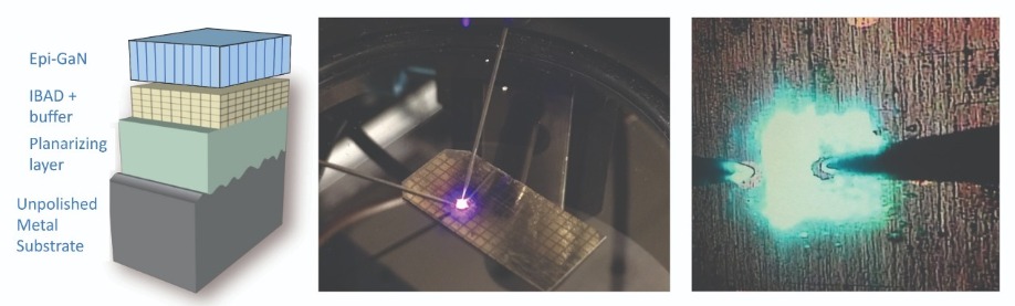
Figure 1. iBeam Materials’ GaN-on-metal technology relies on a single-crystal-like layer that is created on top of a polycrystalline substrate, such as a long-length metal foil. The single-crystal-like layer is formed by an ion-beam-assisted deposition process. On the left is shown the layer architecture, while photographs show the first LED devices.
Making displaysWith the conventional approach to making large-area microLED-based displays, there is a need to use a high-yield process that provides massively parallel transfer of individual LED chips that may be less than ten microns in size. High-definition displays contain 1080 by 1920 pixels, so they require 6.2 million red-green-blue subpixels. And in a 4K display, there are nearly 25 million subpixels. These numbers are so high that in order to minimize the number of transfer steps, LEDs have to be transferred in many thousands at a time.
Several companies are developing technologies for handling in parallel such large groups of LEDs, which could have dimensions down to just 3 μm. These approaches have to transfer chips with micron-scale precision, bond them reliably, and realise an incredibly high yield. Even 99.99 percent will not be good enough, as the display could still contain thousands of dead subpixels. They would have to be repaired, because the market will not tolerate even a single malfunctioning or missing pixel in a new device.
Repairing individual pixels is an option, but costs escalate, as this requires additional transfer steps. So it may be better to resort to redundancy in transferring. However, this adds significantly to the LED cost, and it fails to address the problem head-on.
In contrast, we tackle this issue with a technology that can make a paper-thin flexible product with a resolution of 500 pixels per inch or more, and satisfy the market’s tremendous desire for integration of displays into thin, curved devices. Using patented GaN-on-metal technology, we grow LED-quality InGaN material directly onto low-cost, large-area flexible metal foil, making monolithic integration of microLEDs practical.
This foil allows our displays to be as good as or better at conforming to curved surfaces than OLEDs. In addition, they may even be able to flex when in use. The conformable metal substrate also provides reflectivity and heatsinking for the LEDs (see Figure 2).
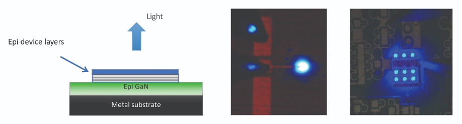
Figure 2. Diagram of an LED cross section, and emission from a 20 μm blue LED on metal and an array of microLEDs
Our technology is compatible with a roll-to-roll process, which, alongside new epitaxial methods that will supersede MOCVD, will slash the cost of manufacturing microLEDs. Currently, costs for MOCVD wafer production are in the range of$2-3/cm2, but they could fall by a factor of three by switching to long-length metal substrate. Further savings will result from the introduction of non-MOCVD deposition processes – our cost model estimates an epi-material cost reduction of more than a factor of ten per unit area (see Figure 3).
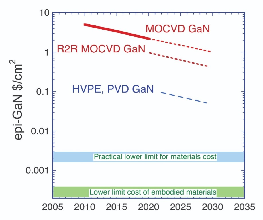
Figure 3. Cost curves of epi-GaN device layers for various deposition methods.
Ultimately, LED costs could fall to less than 10 cents per cm2. Such a dramatic reduction could allow microLED displays to be even cheaper than those based on OLEDs.Fabrication of our full-colour, active-matrix display begins by producing a dense array of blue-emitting LEDs monolithically across the surface of the epilayers. Each pixel comprises three sub-pixels, with red and green components formed by coating blue-emitting elements with quantum-dot down-converting layers (see Figure 4). They can be added as a photoresist matrix, or with an inkjet printer, depending on the size of the LEDs required.
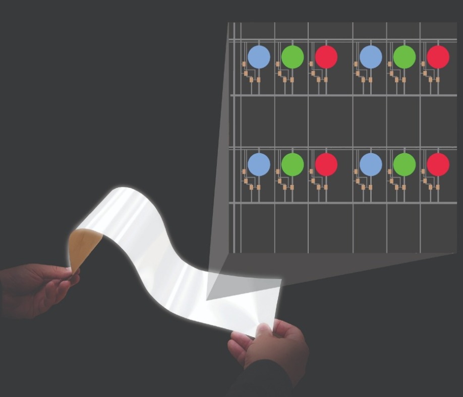
Figure 4. The layout of a microLED display made using iBeam technology.
The next step is to add a thin-film transistor circuit to address each of the sub-pixels. We are able to draw on the existing backplane technology used to make OLED displays, with thin-film materials deposited on the sheet, prior to patterning (see Figure 5).
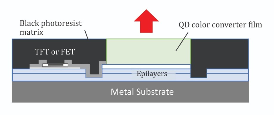
Figure 5. A sub-pixel cross-section showing a quantum-dot, colour-converting film and black photoresist matrix.
The total thickness , including that of the metal substrate, can be less than 100 μm. To reduce crosstalk, quash stray emission and realise better blacks, the spaces between the LEDs can be filled with a commercially available black polymer matrix.Our technology will continue to advance. In future, we will use the epitaxial GaN sheet that exists on the metal foil to fabricate small, integrated GaN transistors. These devices can be used to control the LEDs (see Figure 6).
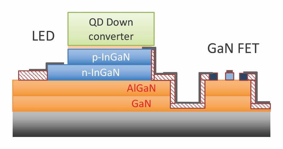
Figure 6. The sub-pixel LED can be integrated with an GaN/AlGaN FET transistor device, by integrating the FET in the epi structure.
By adopting this approach, we are following in the footsteps of the silicon industry. It famously evolved from making circuits by individual wiring of discrete transistors to the high-yield manufacture of highly integrated circuits with billions of transistors on a single chip.We are confident that over time, the yield and reliability of microLED displays made with our technology will be far higher than those made with chip-transfer methods. However, to begin with, it may be prudent to utilize some redundancy in design, in order to minimize possible LED failure.
When there is a move to higher-resolution displays, our technology is well-positioned – thanks to the complete area being filled with LED epi, higher resolution displays can be made with smaller additional costs. For our monolithically integrated LED display technology, cost scales with area, rather than the number of pixels.
Our approach is not the only one providing monolithic integration. One alternative involves nanowire active regions. However, this relies on conventional rigid substrates, such as silicon and sapphire. Go down that path and the manufacture of large-area displays tends to require the transfer and bonding of LEDs to a backplane.
Colour and gamut
The quantum dot technology that we are advocating to make our displays is advancing, with today’s films with a thickness of just a few microns providing nearly full conversion of blue emission to that in the red or green. However, if there are concerns relating to any unwanted blue light that remains in the sub-pixel spectrum, it can be removed with a filter or blue reflector.
Makers of displays can choose the quantum dot films to hit specific colour points. The narrow emission of the LEDs and the quantum dots – they have spectral widths of typically 20 nm and 30 nm to 40 nm, respectively – enables saturated colours, along with colour gamuts that are wider than those of conventional LCDs and OLEDs (see Figure 7 for further details).
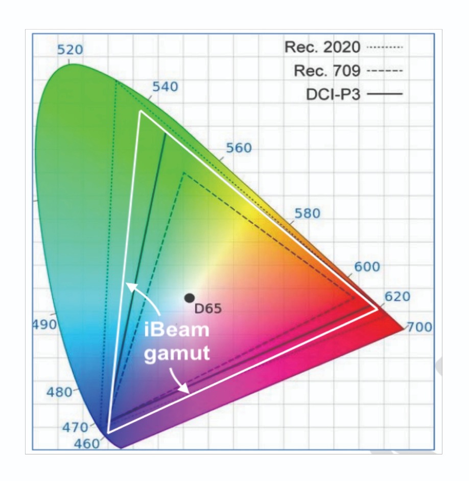
Figure 7. Three popular gamut standards are targets for new products.
Rec. 709, also called sRGB, is the current HDTV standard. However, products such as the Apple iPhone and Samsung Galaxy have already moved to embrace DCI-P3, the digital cinema standard, and future products are targeting the most difficult laser-based Rec. 2020 standard. iBeam technology will be capable of exceeding DCI-P3 and nearly meeting that of Rec. 2020 without requiring lasers.As the microLED market expands, there is a need for a roll-out of significant additional LED manufacturing capacity in order to make all the required displays. By 2026, some forecasts show 15 percent of the 2 billion cellphone market will feature a 4K microLED display. This alone will require 12 million wafer starts per year, a figure comparable to the total for all LEDs that will be manufactured in 2019. Factor in wearables, TVs, and other display formats, and manufacturing volumes are set to be far higher than this figure.
Our low-cost, roll-to-roll capability can make this ramp possible. Just one wide-web, roll-to-roll production facility could equal today’s total worldwide LED epi production.
Beyond 2025, displays based on two-dimensional flat screens are expected to be superseded by those that create images in a three-dimensional space (see Figure 8). This can be accomplished by placing an array of emitters, such as microLEDs, over a microlens array. However, to ensure that the light-field display has a high resolution, in addition to compression of huge amounts of data, it must feature billions of pixels with a pitch that could be as small as 5 μm. Such a colossal number of pixels is impractical for mass transfer approaches, but can be realised with our monolithic integration technology.
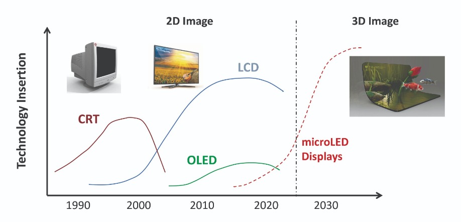
Figure 8. Historical evolution of displays and expectations into the future.
In short, a promising future lies ahead for our technology, which enables the manufacture and integration of microLEDs on large area, metal foils. Wearables, augmented reality, mobile products and even large displays will benefit, due to the many great attributes of our technology. They include: a flexible, light-weight substrate that enables displays to fit curved surfaces and ease of integration into products; the use of direct-emitting LEDs, which allow outdoor viewing and produce a high dynamic range, a wide colour gamut and deep blacks; low cost, due to monolithic integration and compatibility with high-volume roll-to-roll manufacturing techniques; and the promise for light-field displays, the three-dimensional displays of the future.United States Patent 9,735,318 B, V. Matias and C. Yung.
V. Matias, Photonics West Presentation, 2018
Yole Développement, “Are MicroLEDs a credible alternative to LCD and OLED?” SID Display week business conference, (2018)
G-S. Chen et al. IEEE Phot. Tech. Lett. 30 262 (2018)


