


Producing a gallium oxide power portfolio
Gallium-oxide trench-type power devices with novel architectures have the attributes to trump those made from silicon carbide
BY KOHEI SASAKI AND AKITO KURAMATA FROM NOVEL CRYSTAL TECHNOLOGY AND SHIGENOBU YAMAKOSHI FROM NOVEL CRYSTAL TECHNOLOGY AND TAMURA CORPORATION
The days of the internal combustion engine are numbered. Concerns over climate change are encouraging governments to consider banning sales of petrol and diesel vehicles by 2030 or so. And even in those countries that many not enact this legislation, there will be many individuals living there that will be turning to electric vehicles to do their bit for the environment.
Even before the ban, sales of electric cars will climb as they fall in price and deliver an ever better performance, including being able to go further on a single charge. This will be accomplished in part by increasing the efficiency associated with the power system that drives the car. Today, significant losses occur in the semiconducting power devices used to alter the current or frequency of electricity, due to considerable electrical resistance of the components. Trim these losses and the range of the car could increase, tempting drivers to make the switch to a zero-emission vehicle.
The incumbent material for power semiconductors is silicon. Replacing this with the leading alternative, SiC, cuts losses. However, devices made from this wide bandgap material have non-negligible manufacturing costs, and it is difficult to use them in non-industrial applications, such as home electronics and private vehicles.
A far more promising option is the ultra-wide bandgap material gallium oxide, which has a huge critical electric field strength (see “The strengths of gallium oxide” for details of its great material properties). In the form of its β-polytype, it has been used to make incredibly low-loss devices with breakdown voltages of over 600 V. The hope is that one day device fabrication costs will be as low as they are for silicon, because β-Ga2O3 wafers can be made with a melt growth method that is similar to the one used to make silicon wafers. Due to these positive attributes, β-Ga2O3 power devices have great potential for deployment in electric vehicles – there are even plans to start installing them in this class of car by 2025.
The cost of chip production is governed by economies of scale. Larger epiwafers are needed to drive down costs, and our team from Novel Crystal Technology and Tamura Corporation are working towards this. Currently, we are selling 2-inch b-Ga2O3 epitaxial wafers (see Figure 1), and this market is taking off, with sales of this material doubling annually. But as well as building new growth chambers to meet demand, we are also producing larger versions to meet requests for larger wafers. Later this year, we will also start to sell 4-inch β-Ga2O3 epiwafer samples.
In addition, we are preparing for the manufacture of a portfolio of high-performance devices. Read on to learn about the development of our ground-breaking diodes and transistors.
Trench diodes
Special device structures may be needed to explore the full potential of β-Ga2O3. That’s certainly the case with the Schottky barrier diode. Adopt a conventional design and device characteristics are limited by the leakage current at the Schottky junction.
We overcome this limitation with a periodic trench metal-oxide-semiconductor (MOS) structure (see Figure 2). Inserting this trench under the anode electrode decreases the electric field at the Schottky junction, leading to a reduction in the leakage current.
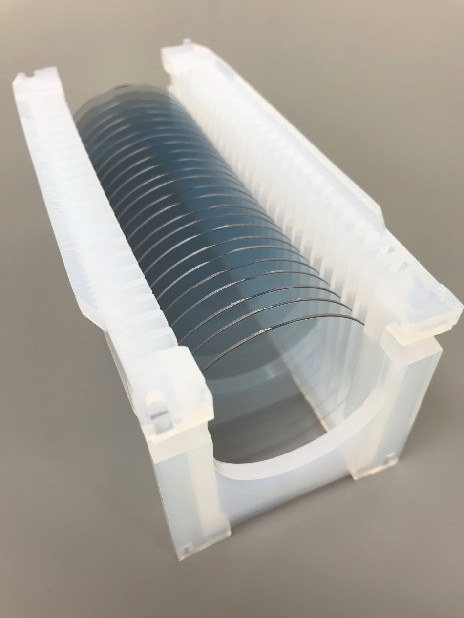
Figure 1. 2-inch single crystal b-Ga2O3 wafers produced by Novel Crystal Technology.
To construct the MOS Schottky barrier diode, we load our β-Ga2O3 substrates into a HVPE chamber and grow epitaxial films of β-Ga2O3. After this, trenches are formed by photolithographic patterning and dry etching, before we turn to atomic layer deposition to cover the sidewalls and bottom of the trench with films of HfO2. Fabrication finishes with the addition of Schottky and ohmic electrodes, made from molybdenum and titanium, respectively.Reverse bias measurements of our MOS Schottky barrier diode reveal that it has a leakage current comparable to that of commercially available SiC Schottky barrier diodes (see Figure 3(a)). The breakdown voltage of our device is only 400 V, because we are still developing our anode edge termination technique. Higher voltages will result from the introduction of guard rings, along with other modifications.
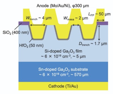
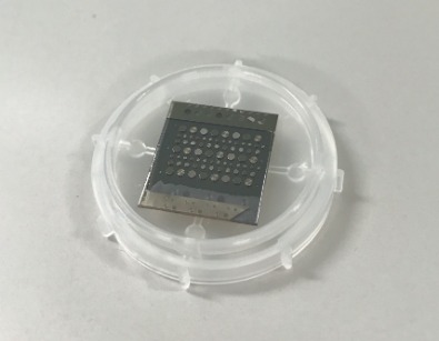
Figure 2. The β-Ga2O3 trench metal-oxide-semiconductor Schottky barrier diode developed by Novel Crystal Technology and Tamura Corporation.
Forward characteristics of our β-Ga2O3 MOS Schottky barrier diodes are more impressive than those of the SiC equivalent (see Figure 3(b)). A threshold voltage that is almost half, combined with an on-resistance that is similar, lead to a forward voltage that is 30 percent to 40 percent smaller. Judged in terms of high-speed operation, both devices are similar.We are confident that when our β-Ga2O3 MOS Schottky barrier diodes are used to replace silicon p-n diodes in power factor correction circuits, boosting choppers and inverters, they will cut the power loss of the system. We are currently developing a device fabrication technique for mass production. Manufacture of a limited numbers of test samples commenced last year, and full-scale production is planned for 2021.
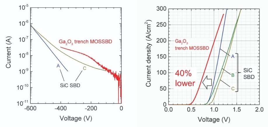
Figure 3. (a) Reverse and (b) forward characteristics of a b-Ga2O3 trench metal-oxide-semiconductor Schottky barrier diode and a commercially available SiC Schottky barrier diode. The b-Ga2O3 device exhibits about a 40 percent lower forward loss than that of the SiC Schottky barrier diode, and has small reverse-leakage characteristics.
Junction barriers
Another option for decreasing the leakage current at the Schottky junction is to embed the p-type region under the anode electrode. This creates a device known as a junction-barrier-controlled Schottky diode, which has similar characteristics to the trench MOS structure that we have just described.
Making this device is not easy, because p-type doping techniques are not available for β-Ga2O3. Our solution is to use a heterojunction, pairing p-NiO with n-Ga2O3.
To ensure success, we had to determine the electrical characteristics of the junction between these two oxides. Knowledge of the breakdown voltage would be crucial to developing a high-performance device. To this end, we fabricated a simple p-n diode by growing an n-Ga2O3 film on a Ga2O3 substrate, before adding p-NiO by RF sputtering. The resulting heterojunction has a high breakdown voltage – it is over 700 V – and good forward characteristics. These are very promising results, given that this p-n junction contains an amorphous film.
Armed with what we have learned, we fabricated β-Ga2O3 junction-barrier-controlled Schottky diodes (see Figure 4 for details of their design). Trenches were formed by dry etching, and filled with p-NiO. To complete fabrication, molybdenum Schottky electrodes and titanium ohmic electrodes were added.
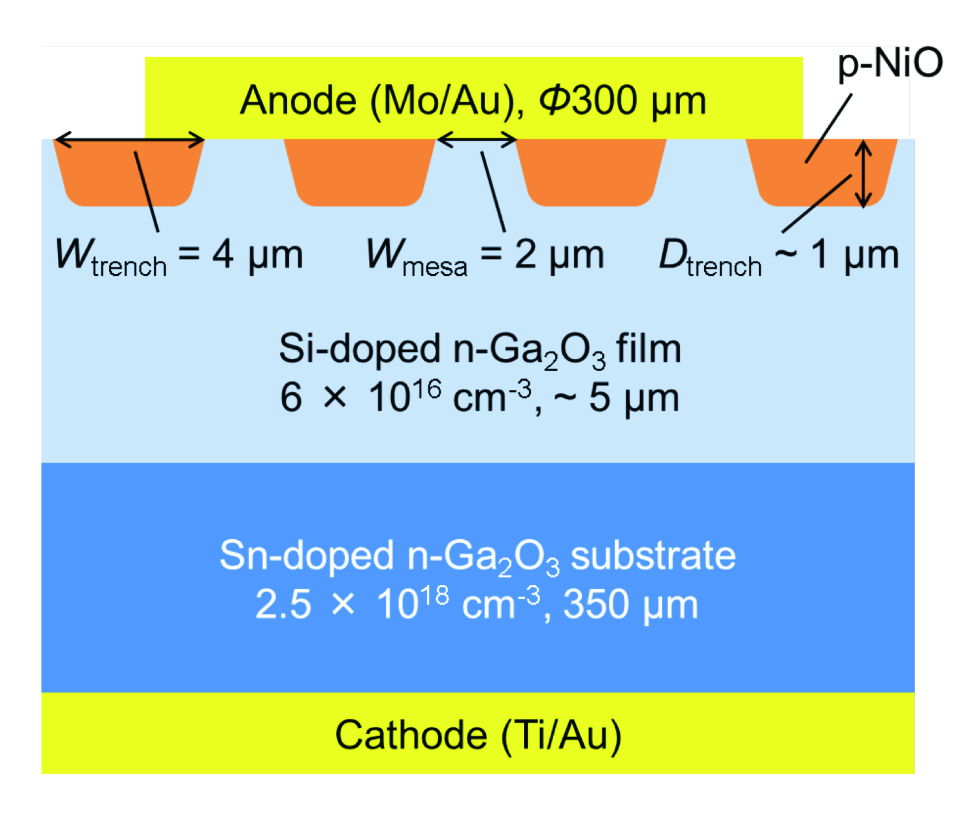
Figure 4. Schematic illustration of b-Ga2O3 trench junction-barrier-controlled Schottky diodes.
We have compared the electrical characteristics of these devices with conventional Schottky barrier diodes, made on the same wafer. Reverse characteristics revealed that the conventional Schottky barrier diode has a large leakage current, while that with a junction barrier has a value that is lower by several orders of magnitude (see Figure 5(a), which also includes the theoretical characteristics of a thermionic field emission current for a normal Schottky barrier diode). Even lower in leakage, though, is the p-n diode, indicating that our junction-barrier-controlled Schottky diode is still to be optimised.When it comes to forward characteristics, the p-n diode is inferior to both the junction-barrier-controlled Schottky diode and the Schottky barrier diode. The latter two have a threshold voltage of 0.5-0.6 V, compared with 2.2 V for the p-n diode (see Figure 5). These results indicate that the forward current of the junction-barrier-controlled Schottky diode flows through the Schottky junction normally.
Even better results should be possible by using the p-NiO/n-Ga2O3 heterojunction to make guard rings that prevent the electric field from concentrating too much at the electrode. These structures are essential for realizing high-breakdown-voltage devices.
Based on the result so far, and the potential for further improvement to the junction-barrier-controlled Schottky diode, we believe that this device has a great future. Its major asset is that it compensates for a major weakness in β-Ga2O3 – the absence of a p-type doping technology. Development is proceeding smoothly, and we are considering mass production.
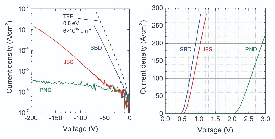
Figure 5. (a) Reverse and (b) forward characteristics of junction-barrier-controlled Schottky diodes (JBS), Schottky barrier diodes (SBD), and a diode with a p-n junction (PND). The black dotted line indicates the calculated thermionic emission current for a normal Schottky barriers diode.
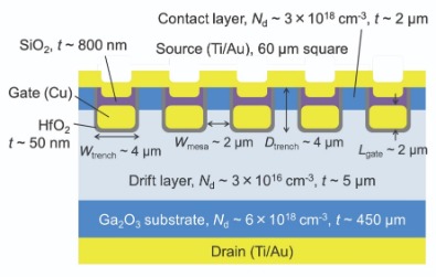
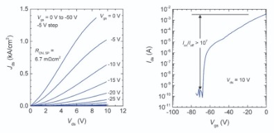
Figure 6. (a) Schematic illustration, (b) current density-voltage, and (c) transfer characteristics of a β-Ga2O3 trench MOSFET.
Power transistors
Our next target is the development of β-Ga2O3 power transistors. Due to the lack of p-type doping, we are working with a static induction transistor-type structure, made from entirely n-type material. A hallmark of this device is that its behaviour can be adjusted from a normally on FET to an off variant by simply changing either the mesa width or the donor concentration in the mesa region.
We have developed a normally on device (see Figure 6 for the device design). This is easier to make than its normally off sibling, simplifying our efforts to demonstrate operation of vertical β-Ga2O3 FETs. We fabricated this transistor using the process developed for trench MOS Schottky barrier diodes.
Measurements on this device reveal a huge current density – it is over 1.3 kA/cm2 – and clear current modulation upon application of a gate voltage (see Figure 6(b)). Transfer characteristics show that the on-off ratio is over 107
Further reading
K. Sasaki et al. IEEE Electron Device Lett. 38 783 (2017)
K. Sasaki et al. ICSCRM 2017, WE.E1.7
K. Sasaki et al. Appl. Phys. Express 10 124201 (2017)
(a) Z. Hu et al. IEEE Electron Device Lett. 39 869 (2018)
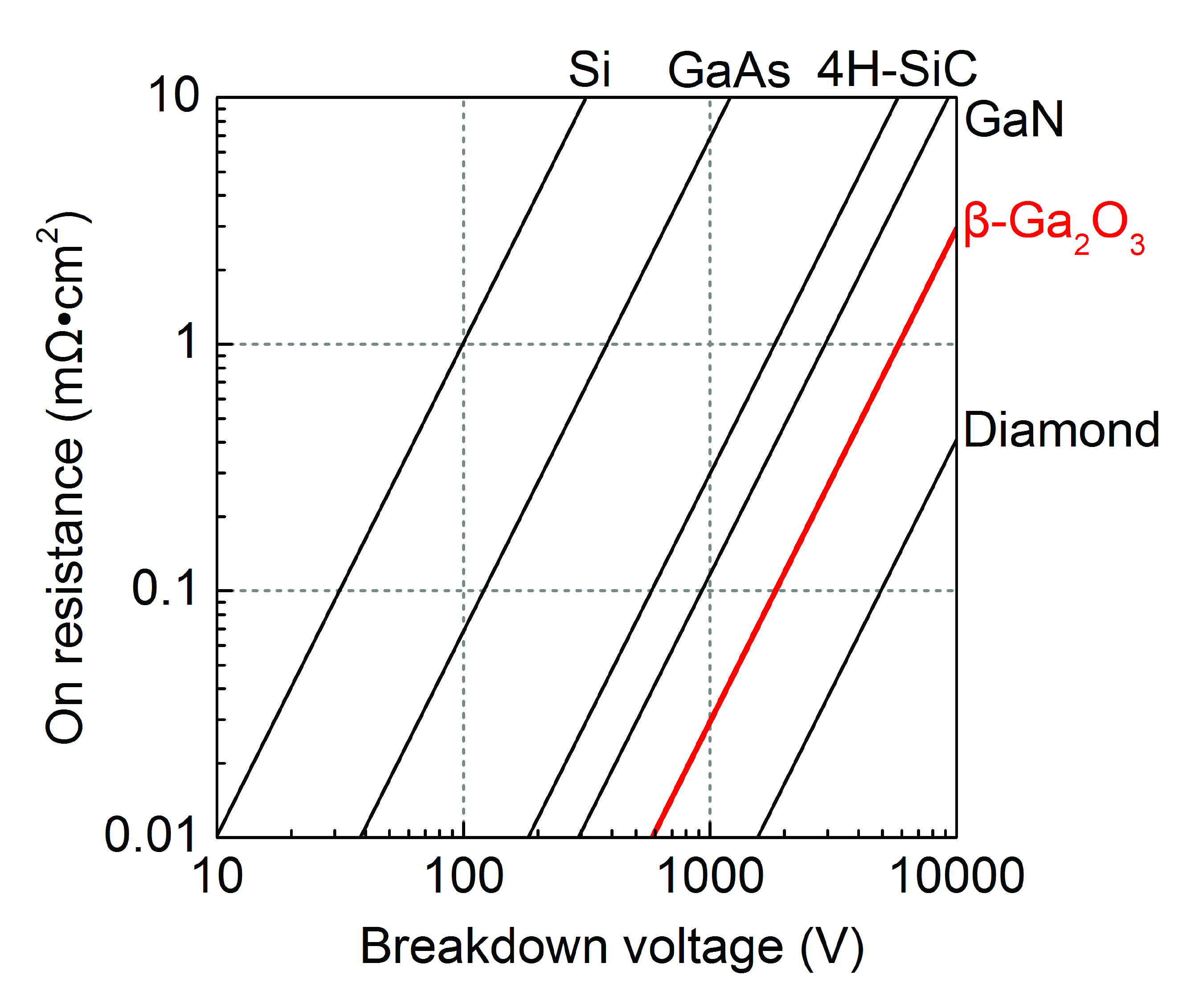
The potential of β-Ga2O3 is highlighted by its value for Baliga’s figure of merit, which is a guide to how suitable a material is for power devices. The figure for β-Ga2O3, calculated from its material properties, is 3,000 times larger than that of silicon and ten times that of SiC.
Behind this high figure for β-Ga2O3 is its extremely large bandgap – it is about 4.5-4.8 eV. This figure offers an estimate of the critical electric field strength of 8 MV/cm (see table below).
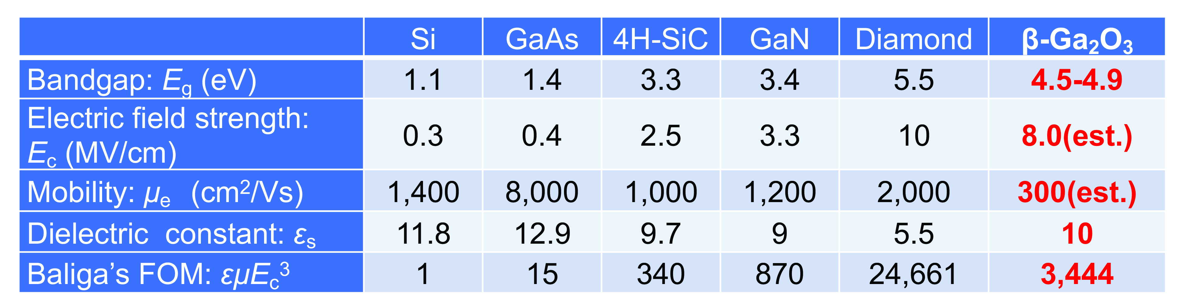
To make devices, there is a need to dope material. The doping concentration in β-Ga2O3 can be controlled over the range 1015-1020 cm-3 by impurity doping, in spite of the large bandgap.
The great potential for β-Ga2O3 power devices is underscored in the plot above. The theoretical limit for the specific on-resistance, illustrated by the solid line, is 3,000 times smaller than that of silicon devices and one-tenth that of SiC devices for the same breakdown voltage.
Another merit of β-Ga2O3 is that large single-crystal substrates can be produced with the melt-growth method. As this growth technology is already used for the manufacture of silicon and GaAs substrates,
it is expected that large, high-quality β-Ga2O3 substrates can be easily manufactured at low cost.
Theoretical specific on-resistance as a function of breakdown voltage. The solid lines indicate the theoretical limit, determined from the material properties.