
Combining logic and wireless
Equipping silicon with InGaAs channels improves the logic and high-frequency performance of RF-CMOS
BY CEZAR ZOTA, CLARISSA CONVERTINO AND LUKAS CZORNOMAZ FROM IBM ZURICH
The digital revolution defines our times. We live in the information age, enabled by a huge flow of data – it passes through submarine communication cables, is encoded on high-frequency electromagnetic waves, and flows in and out of computers, which process it with the help of billions of transistors. Today, we not only take it for granted that we have immediate access to information and social networks, but also to continual improvement in all these technologies. We expect smartphones, laptops and personal computers to get faster and more efficient, and to have connectivity at higher rates.
For many years, the development of computers and gadgets kept pace with the shrinking of silicon CMOS technology, via the scaling laws of Robert Dennard. Those rules established a way to miniaturize the silicon transistor, while improving its performance and maintaining chip power density. This has been accomplished by a simultaneous reduction of the supply voltage and key transistor dimensions, such as the gate oxide thickness and the gate length.
Dennard scaling had a good run, starting in the 1960s and continuing all the way to the beginning of this century. But in the end, the physical limits of electron transport have caught up with scaling, through two key phenomena that only hold back highly scaled, modern transistors.
The first of these is that a reduction of the supply voltage, perhaps paradoxically, leads to an increase in the off-current when the on-current is maintained at a constant level, in order to avoid degradation of the processor clock rate. In practice, the supply voltage cannot drop below 0.7 V, which is today’s value in state-of-the-art silicon CMOS finFETs.
The second phenomenon is a trimming of the increase of the on-current with gate-length scaling, due to the device entering the so-called ‘quasi-ballistic regime’ – a carrier transport mode where electrons don’t scatter as they travel through the transistor channel.
Both of these effects have had a profound impact on scaling. This no longer produces an increase in processor clock rate, which has hovered at around 3 GHz for more than a decade. Instead, since 2003, reductions in transistor dimensions have held the key to a higher transistor density and enabled the introduction of multi-core processor architectures.
Another impact of the disabling of the traditional scaling paradigm has been the heralding of an era of developments driven by innovation and material science. Recently, the roll-out of a new technology node has hinged on reductions in dimensions and the introduction of novel device concepts and materials. They have included high-k dielectrics, strained silicon and SiGe, and finFET device architectures.
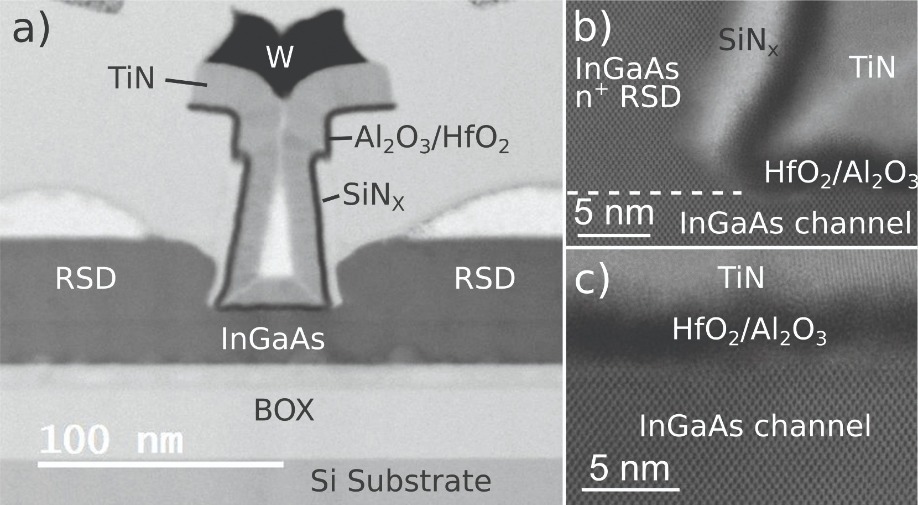
Figure 1. (a) Cross-sectional transmission electron microscopy of a fabricated RF-MOSFET. Close-up on (b) the contact side, showing the raised contact epitaxy as well as the SiN spacers, which reduce parasitic capacitances by separating the contacts from the gate, and (c) the channel region and the gate oxide interface, showing nearly pristine crystal quality of the III-V.
III-V credentials
In this era, there has been much interest in compound semiconductor materials. Their high electron mobilities promise to improve the nFET channel in CMOS technology and boost the drive current in future nodes. For example, InGaAs has an electron mobility six times that of bulk silicon, and could allow a reduction in supply voltage to 0.5 V. That’s a big deal, as it would halve power consumption.
Applications where compound semiconductors are already making a lasting impact include high-frequency technologies, such as radar and wireless communication. Improvements in HEMTs and HBTs have played an important role in the evolution of wireless technology from the fully analogue 1G format of the 1980s to today’s 4G networks. And III-Vs will be an essential ingredient in the roll-out of 5G, which promises peak data rates of 10 Gbit/s and vastly increased network capacity.
The engineers that have developed high-frequency transistor technology have followed different rules from those that advanced silicon CMOS. For starters, scaling is far less critical. Another key difference is that this device employs a semiconductor gate barrier, rather than an oxide. This modification results in a far higher electron mobility. However, this is at the expense of a reduction in electrostatic efficiency, due to the combination of a relatively small dielectric constant and an increase of the gate leakage, stemming from the much smaller band gap of the barrier. The upshot is limited scalability. Progress has instead been driven by device structure optimization, alongside a reduction in parasitic capacitances and resistances, and in particular gate resistance.
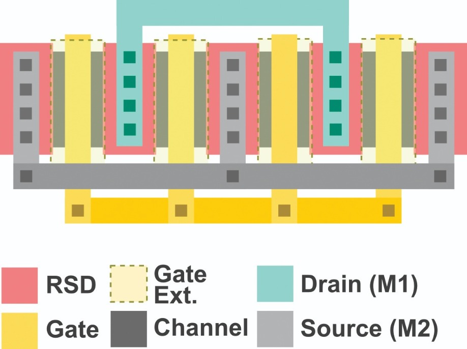
Figure 2. The layout of IBM’s RF-MOSFET with four gate fingers. The gate extension layer indicates an additional metal line on top of the gate metal to reduce the gate resistance.
For III-V high-frequency transistors, the two key performance metrics are the cut-off frequency, fT, and the maximum oscillation frequency, fmax – they are the maximum frequencies for realising current gain and power gain, respectively. Both these values have steadily climbed since the middle of the last century, but since the start of this decade they have stagnated, with ft stuck at around 650 GHz and fmax not going beyond 1200 GHz.There are two reasons for this, both associated with the semiconductor gate barrier. Firstly, due to insufficient electrostatic control, gate-length scaling is inefficient. Secondly, it is not possible to scale down the gate barrier thickness. Doing this increases gate leakage, so increasing oxide capacitance is not possible. This limits the peak transconductance, which directly influences ft and fmax.
The solution to both these issues is to replace the semiconductor gate barrier with a high-k gate oxide. For the last ten years, much effort has been devoted to this, focusing on the demonstration of high-frequency III-V MOSFETs. To date, they lag HEMTs by about a factor two in ft and fmax, primarily due to reduced mobility that arises from electron scattering off of defects in the gate oxide. Nevertheless, the MOSFET outperforms the HEMT in transconductance, due to improved scalability. In particular, MOSFETs from MIT show great promise, reaching 3.45 mS/μm. The potential of these devices could be unlocked with their implementation in a high-frequency compatible architecture.
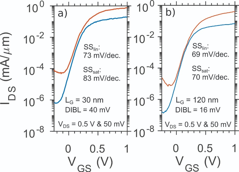
Figure 3. Subthreshold characteristics for short and long-channel finFETs for logic applications. The tri-gate architecture of the finFET improves electrostatic control to reduce the off-current at the intended bias point.
Higher frequencies
The concept of a high-frequency MOSFET is certainly not novel. Within the silicon CMOS industry, there is a class of technology called RF-CMOS. The basic premise is the tweaking of state-of-the-art silicon CMOS technology nodes, so that devices can serve both high-frequency and logic applications.
This dual functionality has many merits. It is lower in cost than III-V HEMT technology, which requires III-V substrates and expensive crystal growth methods. What’s more, by combining RF and logic, this technology allows for tight integration of the likes of wireless communication functionality and digital signal processing. Thanks to this, there can be reductions in delays and form factors, much valued by today’s mobile industry.
However, silicon technology is still held back by the inferior mobility of this material. For example, Intel’s 22 nm RF-CMOS fiFET low-power technologies are limited to 230 GHz and 284 GHz for ft and fmax, respectively.
Given this limitation, it is attractive to integrate III-Vs with RF CMOS technology. While the hike in drive current offered by InGaAs at length scales of 5 nm CMOS and below might not fully compensate for the cost of integrating the III-V channel, the large boost in RF performance could tip the scale in III-V’s favour.
It is not easy to unite III-Vs with RF CMOS. The challenges include how to make high-performance III-V transistors with a silicon CMOS-compatible process flow that is as close as possible to standard fabrication technology, and the key issue of how to integrate III-V channels on silicon substrates. In addition, there is the need to co-optimize logic and high-frequency devices in one technology.
At IBM Research Zurich we have broken new ground by recently succeeding in this endeavour. Our approach involves integrating InGaAs channels on silicon via direct wafer bonding. We cap both a target silicon wafer and a source III-V wafer, which contains the channels, with a bonding oxide that provides adhesion. Both wafers are brought together, and annealing and subsequent stripping of the source wafer leaves a thin III-V layer on an oxide layer on silicon.
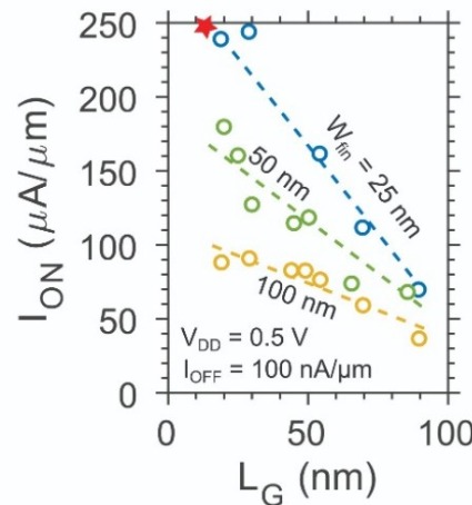
Figure 4. Comparison of the on-current, defined at a specific supply bias and off-current, for various gate lengths. The red star indicates IBM’s previous results at IEDM 2017, for a solely logic-suitable technology. With IBM’s latest technology, a similar logic performance is realised while also implementing high-frequency functionality.
Direct wafer bonding has come on in leaps and bounds during the last decade. It is now the leading candidate for III-V integration, because it addresses several key challenges. It is capable of large-area wafer bonding, reusability of expensive III-V substrates, bonding to pre-processed wafers, and the integration of nFET- and pFET-suitable channel layers.There is still room for improvement, as the bonding defect density needs to be reduced to ensure the high mobility of the III-V layers. However, there is no doubt that direct wafer bonding has matured into a technology facing imminent industrial use.
One of the strengths of our III-V RF-CMOS technology is that it employs a fully silicon CMOS compatible process flow. Processing includes a gate-first high-k/metal gate flow, producing self-aligned source and drain regions that are raised and in situ doped, as well as a palette of silicon-compatible materials. By taking this approach, we highlight the possibility of a cost-effective introduction of III-Vs in a silicon technology. Added foundry costs are minimal.
We have used our process technology to make finFETs with 20 nm-wide InGaAs fins. Benchmarking performance against III-V-on-silicon at a competitively scaled gate length – including a comparison with
our platform just targeting logic, reported at IEDM 2017 – reveals that our latest transistors are on a
par with the state-of-the-art. This evaluation is based on a drive current of 250 mA/μm, realised for a fixed off-current and a supply voltage of 0.5 V.
Our latest chip also features RF-MOSFETs. Simultaneous delivery of impressive high-frequency and logic performance results from SiN source and drain spacers that trim the overlap capacitance to the gate electrode, and source and drain contact extensions underneath the spacers. Note that simply adding spacers to reduce parasitic capacitance and thus improve high-frequency performance is not good enough, as this also degrades logic performance by introducing large access resistors in the ungated parts of the channel under the spacers. We avoid this with a novel approach that involves a controllable etch of a small cavity under the spacers, followed by a refilling with a low-resistive contact material that reduces the impact of access resistors.
Armed with this architecture, our InGaAs RF-MOSFETs are capable of an ft of 400 GHz – this is the highest value reported so far for a III-V RF-MOSFET. Following optimisation of our device layout, we obtain a balanced performance of 215 GHz for ft and 300 GHz for fmax. These values are close to the performance of silicon RF-CMOS from Intel and GlobalFoundries.
Higher frequencies are possible. Capacitances are still limiting high-frequency performance, and improvements could be realised with thicker spacers and longer contact extensions. Another refinement is the introduction of a thin quantum well in the channel. This will lead to a hike in mobility, by reducing scattering at both the gate and back oxide interfaces. Making these changes should propel our technology from matching the performance of state-of-the-art silicon equivalents to outperforming them by a considerable margin – and ultimately making a strong case for the integration of III-Vs and silicon.
This work was funded by Horizon 2020 grant agreement no. 688784 (INSIGHT).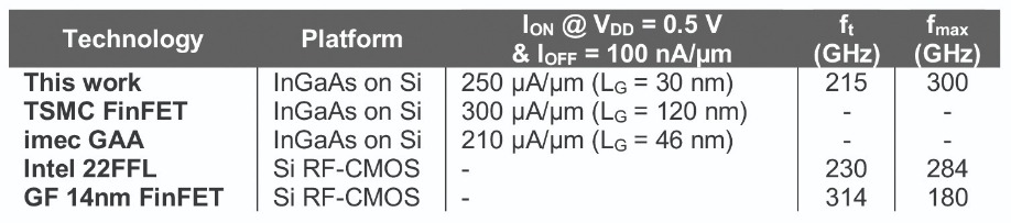
Table 1. A benchmark for various III-V-on-silicon technologies as well as state-of-the-art silicon RF-CMOS. Comparing the high-frequency performance, our new work shows III-Vs for the first time matching silicon RF-CMOS.
Further reading
H. Hahn et al. IEDM Tech. Dig. 17.5.1-17.5.4 (2017)
B. Sell et al. IEDM Tech. Dig. 685 (2017)
C. Zota et al. VLSI Techn. Symp. T15-5 (2018)


