

Invisible Contacts
Transparent GaN circuits are on the horizon, thanks to transfer processes for shifting the transistors onto glass, and the creation of see-through contacts, based on indium tin oxide and ion implantation
BY ZHIHONG LIU FROM SINGAPORE-MIT ALLIANCE FOR RESEARCH AND TECHNOLOGY, GEOK ING NG FROM NANYANG TECHNOLOGICAL UNIVERSITY AND EUGENE FITZGERALD FROM MASSACHUSETTS INSTITUTE OF TECHNOLOGY
Ever more effort is being devoted to the development of invisible electronic circuitry and optoelectronic devices. This field, known as either transparent electronics or see-through electronics, promises to spawn many new products and businesses. To name but a few, it could lead to: smart wind shields in automobiles, smart building windows, transparent flat panel displays, and see-through solar cell panels.
A key component in many transparent electronic systems is this transistor. Today, this device is often in the form of a thin-film transistor, made from a transparent conductive oxide, such as In2O3, ZnO2 or SnO2.
Unfortunately, the performance of those thin-film transistors is vastly inferior to the more common visible transistors, such as the silicon MOSFET. Inferior intrinsic physical properties are to blame, including the polycrystalline structure, lower thermal conductivity, and lower electron mobility – in In2O3, ZnO2 and SnO2, the mobility is typically just 100 cm2 V-1 s-1, one quarter of the value of that of silicon. The low mobility hampers the current that is available to transparent transistors. They are held back by a low current, a low speed, and the need to be driven by a high voltage. What is needed are alternative materials for producing transparent, high-performance devices.
Candidates for replacing the conductive oxides include carbon nanotubes, graphene, and two-dimensional transition metal dichalcogenides. But they all have their own weaknesses, which are difficult to overcome in real applications. Carbon nanotubes are held back by agglomeration, dispersion, purification and sorting; graphene is compromised by fabrication issues for yielding high-quality material, and its intrinsic bandgap limit prevents the transistor channel from fully closing; and two-dimensional transition metal dichalcogenides are impaired by carrier mobilities that are typically even lower than those for transparent conductive oxides.
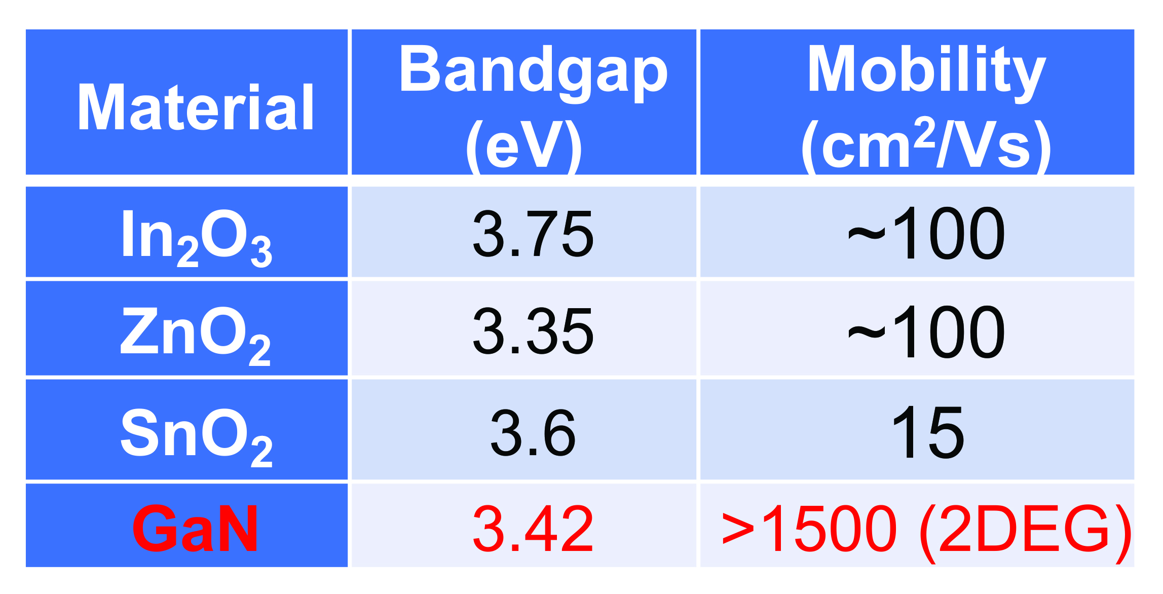
Table I. Comparison of carrier mobilities in transparent conductive oxides commonly used in GaN and in today’s transparent transistors.
At the Singapore-MIT Alliance for Research and Technology, we are pioneering a promising alternative: GaN. From an optical perspective, the bandgap of GaN of 3.42 eV is similar to that of the other contenders (for In2O3, ZnO2 and SnO2, values are 3.75 eV, 3.35 eV and 3.6 eV, respectively), giving GaN an absorption wavelength of 362 nm that enables transparency over the whole visible range. And from an electrical performance perspective, GaN wins hands-down. Mobility is more than double that of silicon in the bulk, and four times that in the form of a two-dimensional electron gas. The saturation velocity is also far higher, as is the critical breakdown field and the thermal conductivity.Hurdles to a transparent transistor
At the heart of a typical GaN transistor is a conducting channel, formed by creating a two-dimensional electron gas at the interface between an AlGaN barrier and the GaN buffer (see Figure 1). This device tends to be produced on a foreign substrate, typically silicon or SiC, and sport three electrodes: a source, a drain and a gate. To ensure transparency, transparent active materials – that is, GaN-based materials – have to be used alongside a transparent substrate and transparent electrodes.
It is not difficult to use a transparent substrate. While a lot of GaN devices are formed by growing nitride layers on an opaque substrate, for example, silicon, there are plenty of transparent options to choose from, including SiC, sapphire, AlN and native bulk GaN. However, all of them are pricey, while the most commonly used substrate for transparent circuits applications – glass – is very cheap.
Our solution is a two-step process that leads to the formation of GaN transistors on glass. Our first step is to deposit GaN materials on a cheap-but-visible silicon substrate, before we transfer the GaN layers onto the glass. Alternatively, we can directly sputter GaN materials on a glass substrate, using a technology developed recently by Hiroshi Fujioka’s group at Tokyo University.
What about the electrodes? Normally, GaN transistors have the pairing of nickel and gold as the gate metal, and employ either a Schottky contact or a metal-oxide-semiconductor (MOS) structure. To ensure transparency, we can modify this design, moving from these opaque metals to a transparent conductive material, such as indium-tin-oxide, which is widely used in transparent electronics. This oxide is a good choice, as it can form a good Schottky contact to the AlGaN/GaN and work as a gate in a GaN transistor. Encouragingly, there are a few reports demonstrating an indium-tin-oxide (ITO) gate in a GaN transistor, and it has been shown that a MOS structure with ITO can also be employed as a transparent gate in a GaN device.
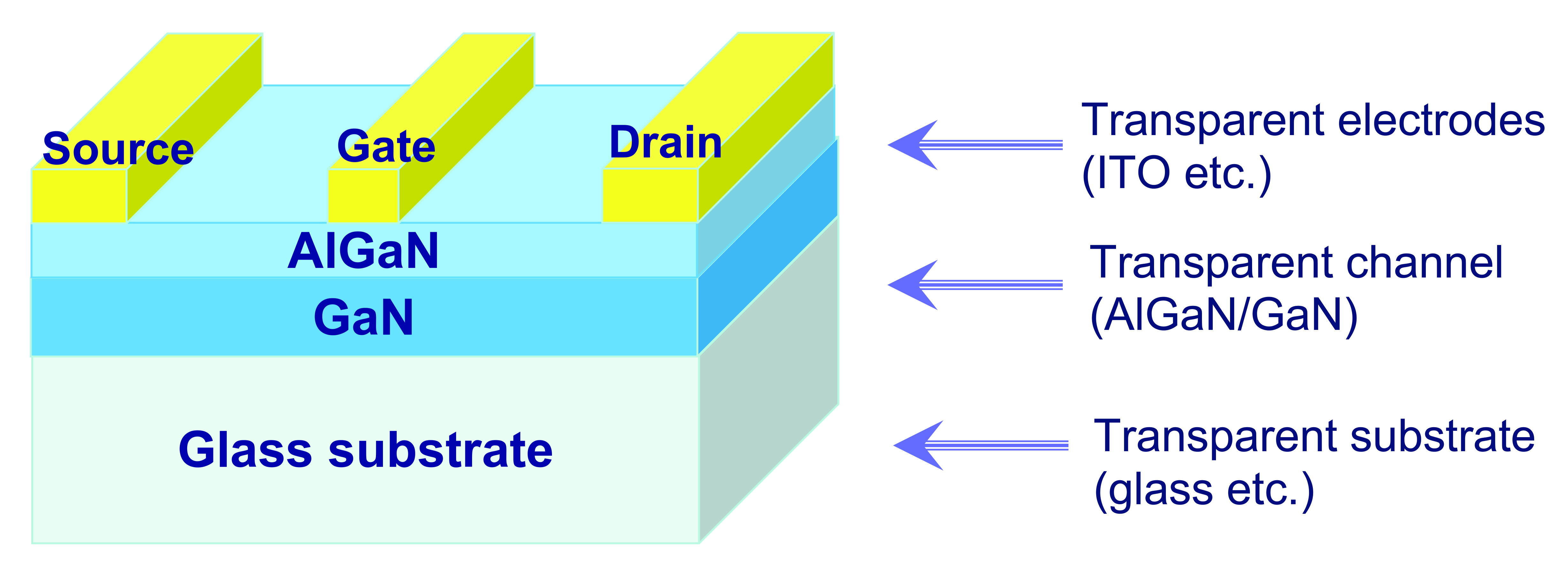
Figure 1. A typical GaN transistor must be modified to form a transparent device.
For the source and drain electrodes, we have to form an ohmic contact between the source and drain material and the channel material. The conventional choice are metals, such as the pairing of titanium and aluminium. Just replacing these opaque materials with ITO is not an option, as the oxide cannot form an ohmic contact with the two-dimensional electron gas (see Figure 2). Note that although upping the annealing temperature increases the current, even at 900 °C, it does not lead to an ohmic contact.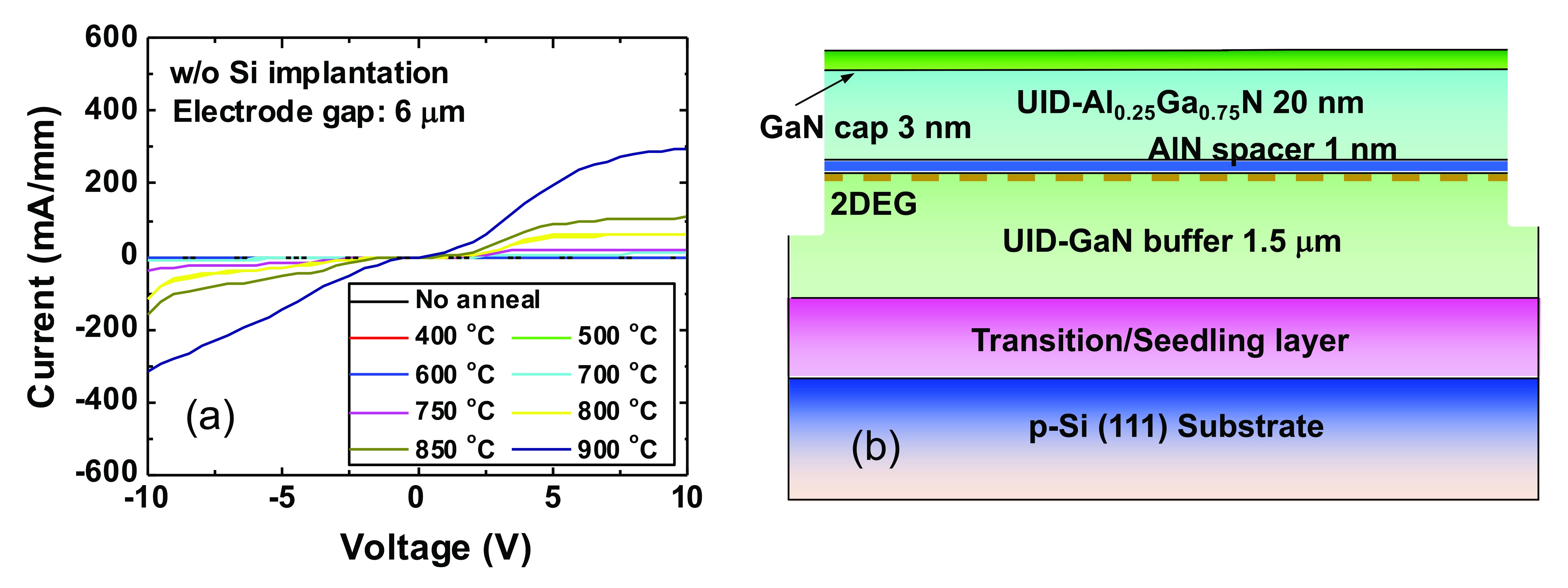
Figure 2. (a) A current-voltage (I-V) curve measured for a pattern with two electrodes made of ITO after different annealing temperatures. The plots show that when the annealing temperature is lower than 600 °C, the current is very small and can be neglected. Increasing the temperature to 700 °C causes current to appear, but ohmic contacts cannot form, even with an annealing temperature as high as 900 °C. The nitride materials in this transistor (b) were grown by the epiwafer supplier IQE, by loading a 200 mm p-type silicon wafer into an MOCVD chamber.
Transparent ohmic contacts…
Simulations of the energy bands reveal why ITO fails to form a good ohmic contact in a GaN transistor. They show that there is a high energy barrier between the ITO and the two-dimensional electron gas at the interface between AlGaN and GaN (see Figure 3(a)). This barrier prevents electrons from travelling smoothly between the ITO and the triangle well in the GaN – and thus prevents the formation of a good ohmic contact. To make one, an approach is needed that pulls down the conduction band of the AlGaN/GaN materials close to the ITO and minimizes the energy barrier (see Figure 3(b)).
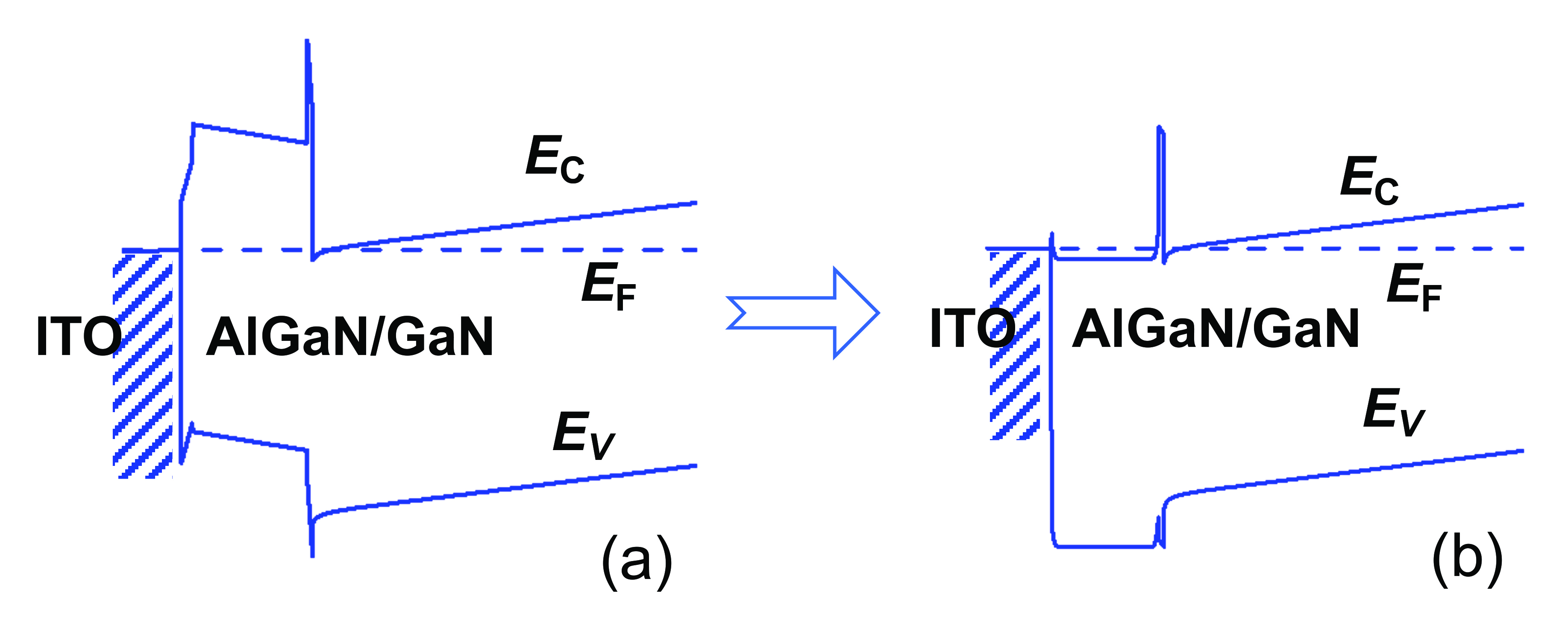
Figure 3. (a) For the energy band diagram for ITO and the AlGaN/GaN heterostructure, there is a high energy level between the ITO and the two-dimensional electron gas (2DEG) at the interface of AlGaN/GaN heterostructure. (b) To form a good ohmic contact, there is a need to pull down the conduction band of the AlGaN/GaN materials close to the ITO and minimize the energy barrier.
One effective approach to pulling down the electron conduction band is to use ion implantation to dope AlGaN and GaN. We have a lot of experience with this, having optimized ion implantation technology to form highly-doped AlGaN/GaN regions and realize good CMOS-compatible ohmic contacts in GaN transistors. Our efforts include the development of an activation annealing method, using ammonia rather than the more common nitrogen to reduce the surface damage during high-temperature annealing of the GaN transistor surface (see Figure 4). By optimising the ion energy, dosage, activation annealing thermal budget and the post-metal annealing thermal budget, we have realised excellent results for the ohmic contact and the sheet resistance of the implanted regions (see Table II).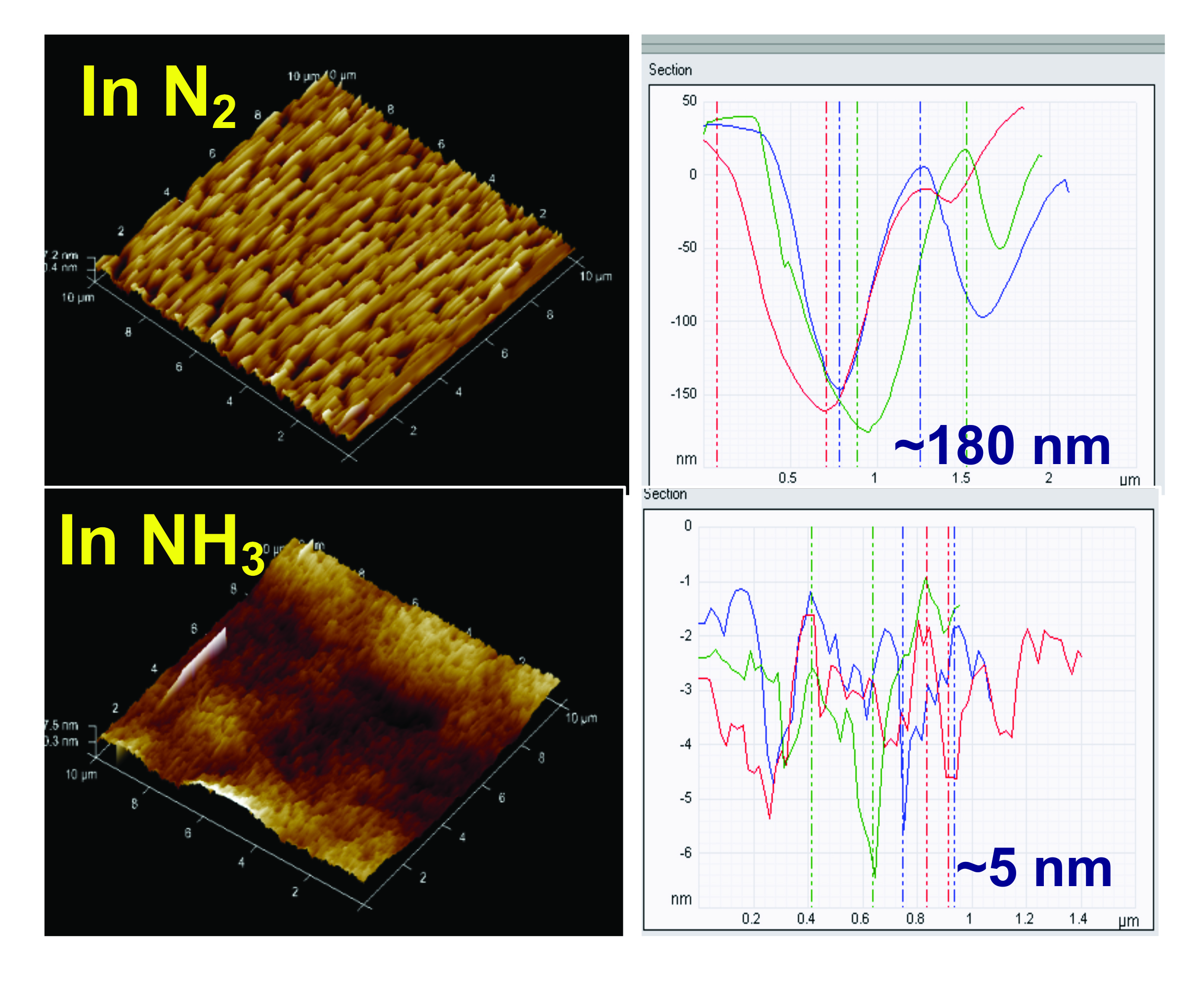
Figure 4. Activation annealing in ammonia can greatly suppress the surface damage caused by high temperature (1200 °C, 2 minutes)
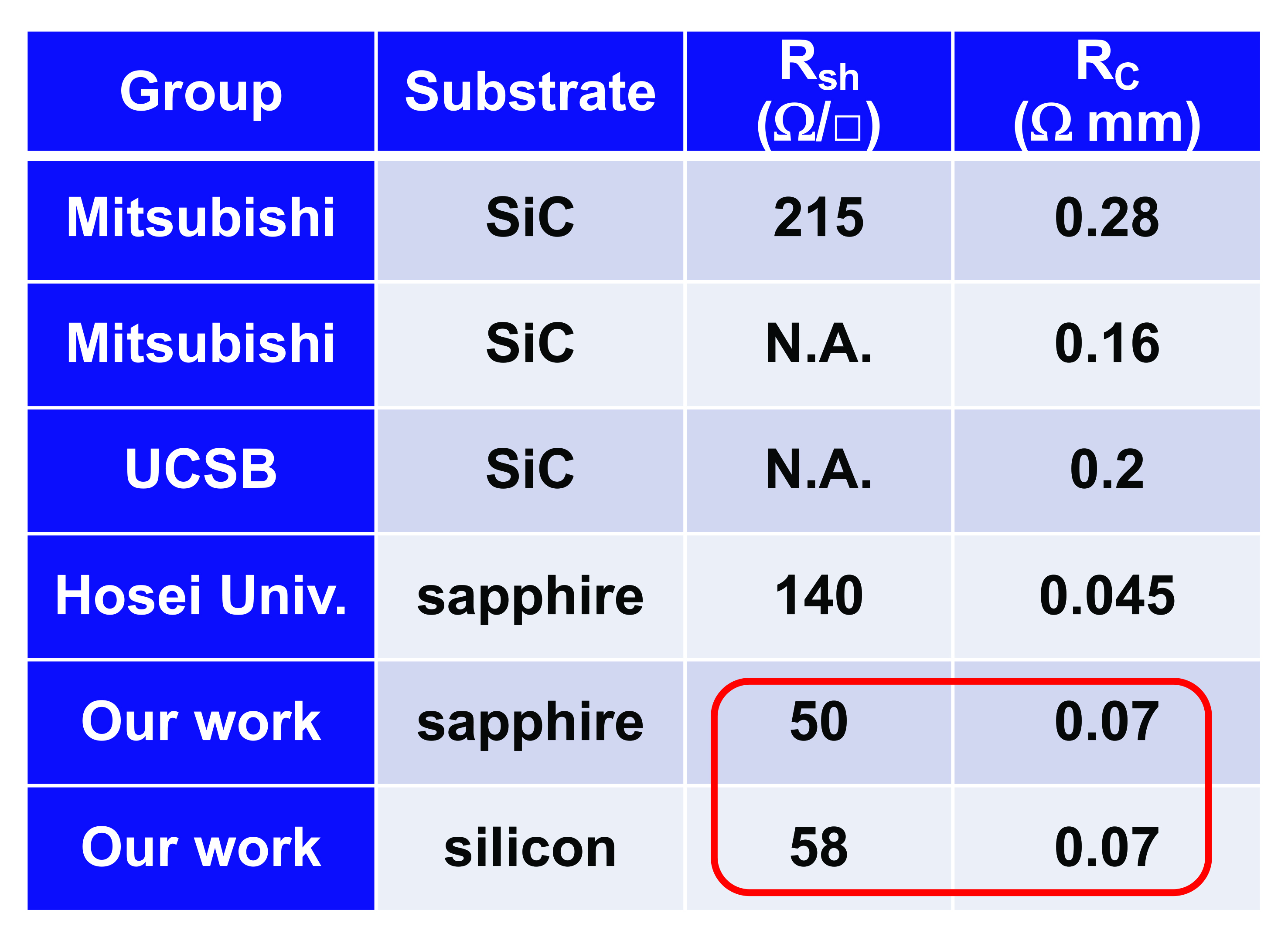
Table II. Excellent results in both sheet resistance (Rsh) of the implanted regions and ohmic contact (RC) have been achieved using silicon ion implantation and CMOS-compatible (Ti/Al metals) ohmic contact technology developed at the Singapore-MIT Alliance for Research and Technology.
More recently, we have transferred these silicon ion implantation techniques to our transparent devices. The implantation conditions that we have adopted are a 30 keV energy, with a 2 x 1015 cm-2 dosage, plus a 80 keV energy with a 2 x 1015 cm-2 dosage, at 7° tilt, using a 300 nm layer of SiO2 as a hard mask for protection. This is deposited by PECVD. We activate the silicon ions by heating to 1200 °C for 5 s in an ammonia atmosphere. The last step is the sputtering of an ITO film, followed by annealing in a nitrogen atmosphere.This approach can form good ohmic contacts between the ITO and the silicon-implanted AlGaN/GaN heterostructure (see Figure 5). Note that good ohmic contacts are even formed when annealing at just 400 °C. Recall that this is in stark contrast to the lack of any current in samples without silicon implantation that are annealed at temperatures below 600 °C (see Figure 6). So there is no doubt that silicon implantation is highly beneficial for the formation of ohmic contacts between ITO and GaN materials.
… and working transistors
To test our approach, we have applied our transparent source and drain ohmic contact technology to real GaN transistors, which use the design shown in Figure 1. In these devices, the two-dimensional electron gas Hall density and mobility are about 8 x 1012 cm-2 and 1500-1600 cm2 V-1s-1, respectively. The ITO ohmic contact is formed with the assistance of silicon ion implantation, followed by annealing under nitrogen for 1 minute at 600 °C.
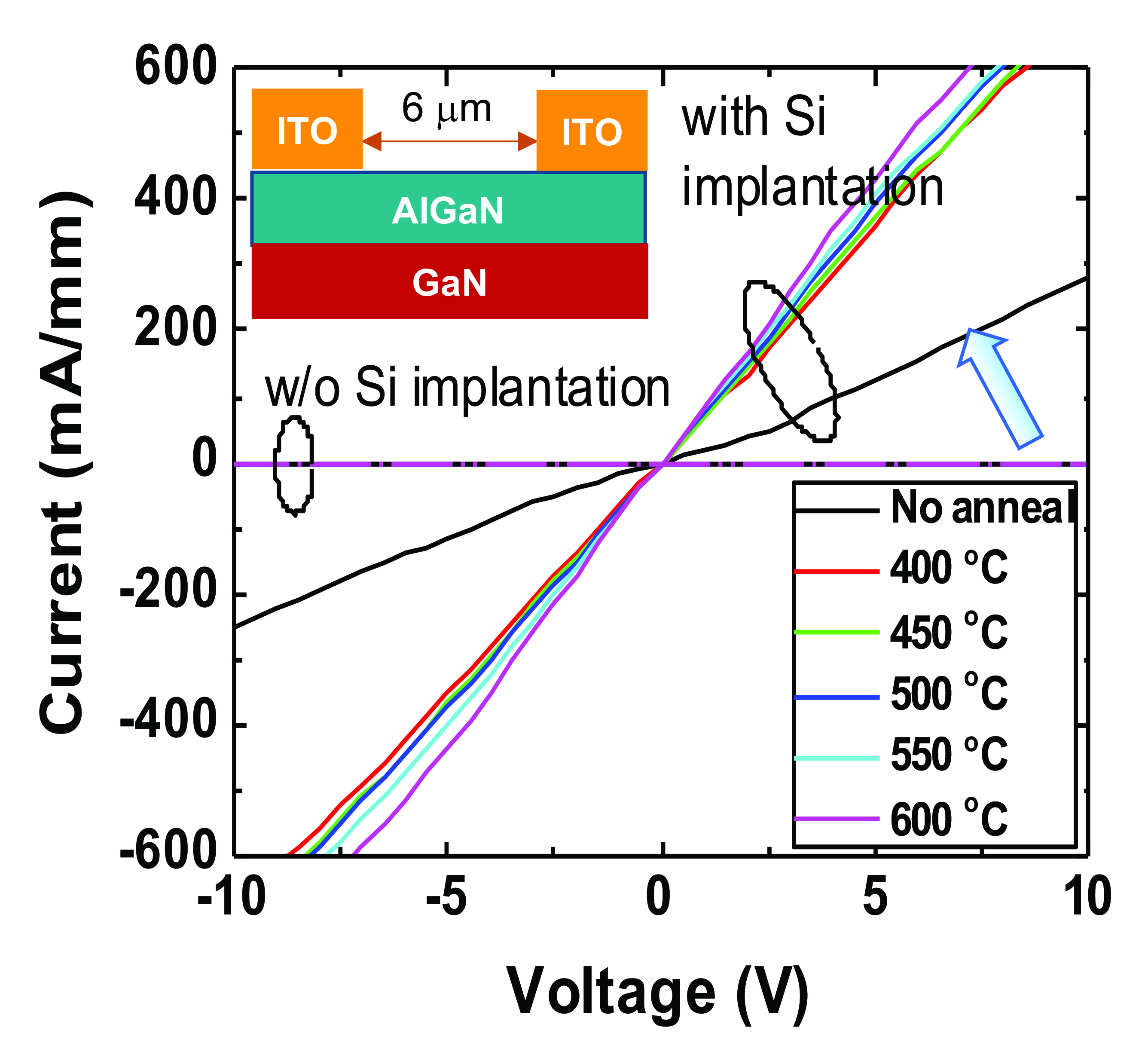
Figure 5. Good ohmic contacts were formed between ITO and the silicon implanted regions in the AlGaN/GaN heterostructure.
DC tests on our devices show excellent results, highlighting the potential that GaN has to be applied in tomorrow’s future transparent electronic systems. Our transistors, which have a gate-to-source distance of 1.5 µm, a gate length of 2 µm, and a gate-to-drain distance of 9.5 µm, exhibit a maximum drain current of 602 mA/mm, a maximum transconductance of 121 mS/mm and a threshold voltage of typically -3.0 V. These values are similar to those found in devices with conventional metal electrodes, indicating that the ITO gate and fabrication process does not introduce obvious extra charges on the device surface. The Schottky barrier height between ITO and AlGaN/GaN is 0.7 eV, which is a little higher than 0.62 eV, a value reported elsewhere.Our work underscores the potential of transparent GaN transistors. To spur their development, we will now try to further optimize the transparent ohmic contact and reduce the contact resistance. This should lead to fully transparent GaN transistors with excellent RF or power performance, and ultimately enable the production of GaN transparent circuits and systems.
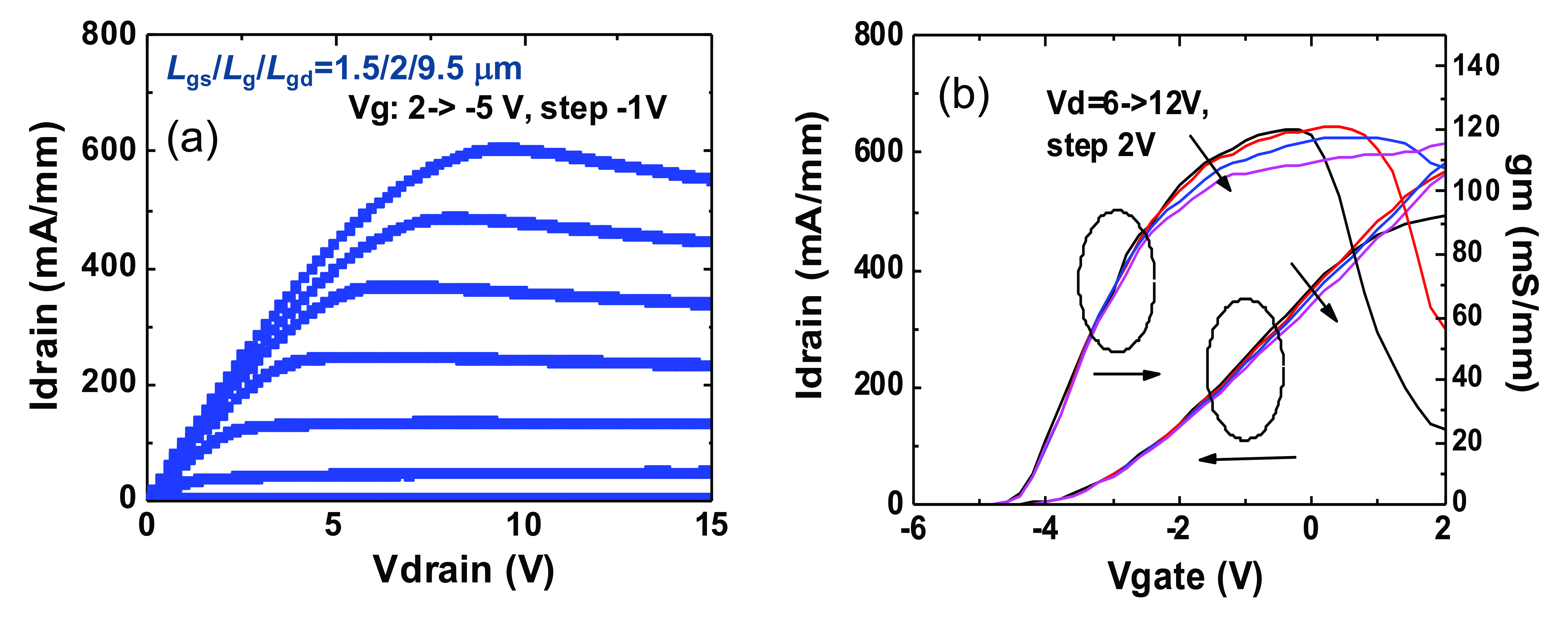
Figure 6. Measured DC performance including (a) output (b) characteristics of a GaN transistor with ITO source/drain (S/D) and gate electrodes.
Further reading
Z. Liu et al. Proc. of IWN, 2018
B. Lu et al. Electron. Dev. Lett. 31 951 (2010)
T. Itoh et al. Sci. Reports 6 29500 (2016)
Z. Liu et al. Proc. of IWN, 2016


