

Scrutinising SiC epilayers
Careful control of the growth process limits the carbon vacancies that govern the carrier lifetimes, but some extended defects and point defects in epilayers are determined by the substrate quality
BY Birgit Kallinger FROM Fraunhofer IISB
Lying at the very heart of every SiC power device is a stack of homoepitaxial layers. Each of them has a carefully selected doping concentration profile and thickness, because this determines the key characteristics of the chip: its blocking capability and its on-resistance.
Unfortunately, these homoepitaxial layers can inherit many forms of extended defects from the substrate, including dislocations and stacking faults, which may hamper device yield and reduce reliability. So how do variations in substrate quality influence the epilayers? And can the substrate quality also influence the point defect concentration, and ultimately the carrier lifetime of homoepitaxial layers and devices?
Working on the answers to these important questions, and related issues, is our team from Fraunhofer IISB, MOCVD manufacturer Aixtron, and Intego, a producer of metrology equipment. Using 100 mm and
150 mm diameter 4H-SiC substrates from a variety of vendors, we have grown SiC epilayers by CVD
and scrutinised the resulting material. This work sheds new light on concerns over wafer quality that are common within the SiC industry – many of those that work within it know that there is a specific defect signature for each vendor, associated with the densities and lateral distributions of dislocations and stacking faults.
Extended defects
Common dislocations in SiC substrates include threading edge or screw dislocations, which lie nearly perpendicular to the surface (along the [0001] c-axis); and basal plane dislocations, which are orientated almost parallel to the wafer surface on the c-plane (compare Figure 1).
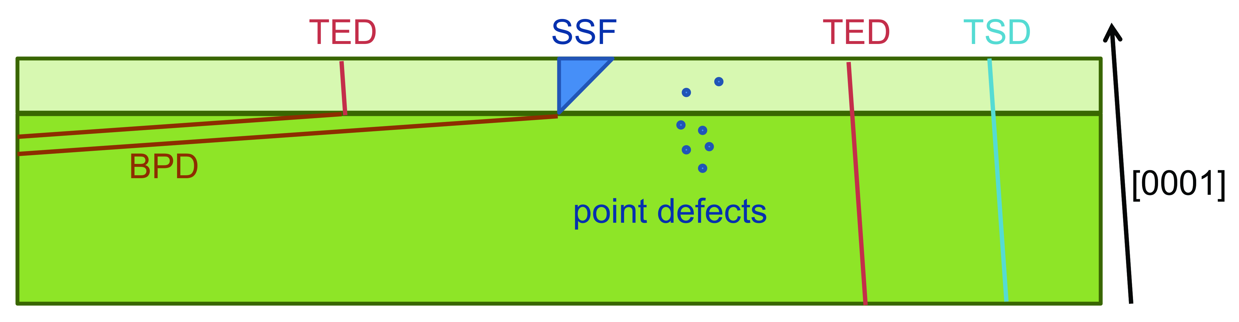
Figure 1. SiC substrates and epiwafers contain many forms of defects, including point defects, stacking faults (Shockley stacking fault, SSF), and various types of dislocations, including: the basal plane dislocation, BPD; the threading edge dislocation, TED; and the threading screw dislocation, TSD
During epilayer growth, the threading dislocations in the substrate tend to make their way into the epilayer. Some threading screw dislocations convert to Frank-type stacking faults, and some to stacking fault complexes like carrots and comets. Fortunately, engineers don’t have to worry about these threading dislocations in the epilayers, as they are harmless in most forms of power electronic device. Stacking faults, however, are a major concern, as they impair device performance and reliability.The most notorious defect is the basal plane dislocation. It can propagate into the epilayer, where it is transformed into a Shockley-type stacking fault or a threading edge dislocation. The former is a menace, causing severe degradation in bipolar devices. Due to this, great strides can be made by uncovering the origins of the stacking faults in these epilayers, and devising appropriate ways and means to minimize their presence.
Motivated by this goal, we have recently turned our attention to comparing the density of triangular-shaped stacking faults in epilayers with the density of dislocations in the underlying substrates. To do this, we have exposed these stacking faults with ultra-violet photoluminescence imaging. This technique produces images with darker and brighter triangles than their background, and features triangular defects with both bright and dark regions – so-called mixed triangles. By inspecting these images, we can see that the triangular shape of the stacking faults in the epilayers originates from the off-axis growth and the hexagonal symmetry of 4H-SiC. We have also undertaken defect-selective etching of reference wafers, to determine the dislocation densities of the underlying substrates (see Figure 2).
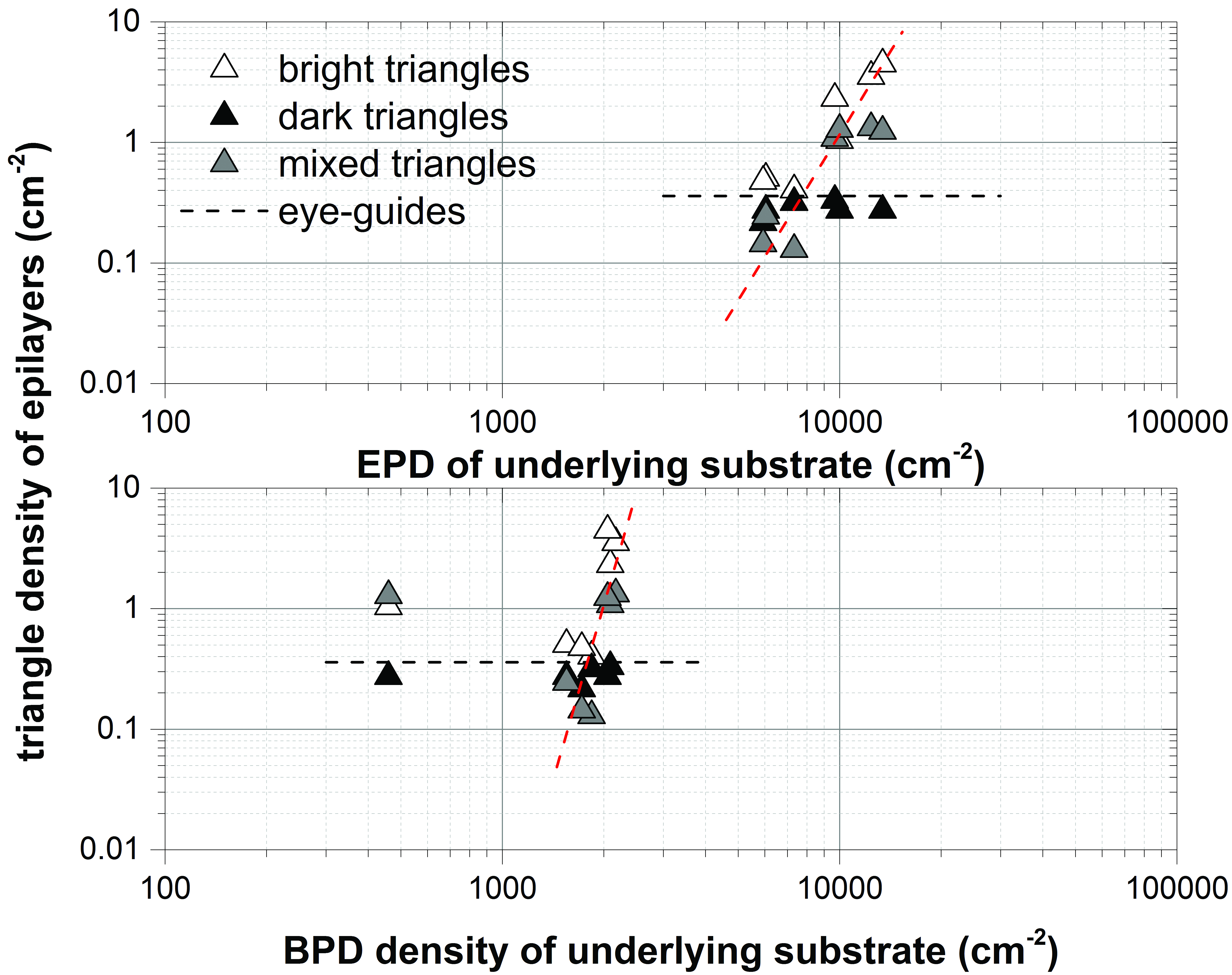
Figure 2. The densities of triangular-shaped stacking faults (“triangles”) in 4H-SiC epilayers and the dislocation densities in the underlying substrates. The triangle densities of epilayers were determined with ultraviolet photoluminescence imaging, while the dislocation densities of underlying substrates were interpolated from defect selectively etched reference wafers.
The densities of the bright and mixed triangular defects appear to be related to the dislocation density of the substrate. This implies that these triangular defects originate from either basal plane dislocations or threading screw dislocations in the substrate. However, for dark triangles, their density is independent of the dislocation densities in the substrate. That’s because the dark triangles originate from ingrown particles, which can be controlled in the epitaxial growth process.There is still more work to do. Our plan is to undertake a further, more detailed investigation of the densities and the origin of extended defects in epilayers, using a pair of new lab tools: an X-ray topography tool XRT Micron from Rigaku, and an ultra-violet photoluminescence imaging system from Intego, equipped with surface inspection. Armed with the insights these instruments will bring, we aim to identify the critical defects for high-quality, reliable devices. This should lead to guidelines for acceptable defect densities for substrates on one hand and for optimum epitaxial growth parameters on the other hand.
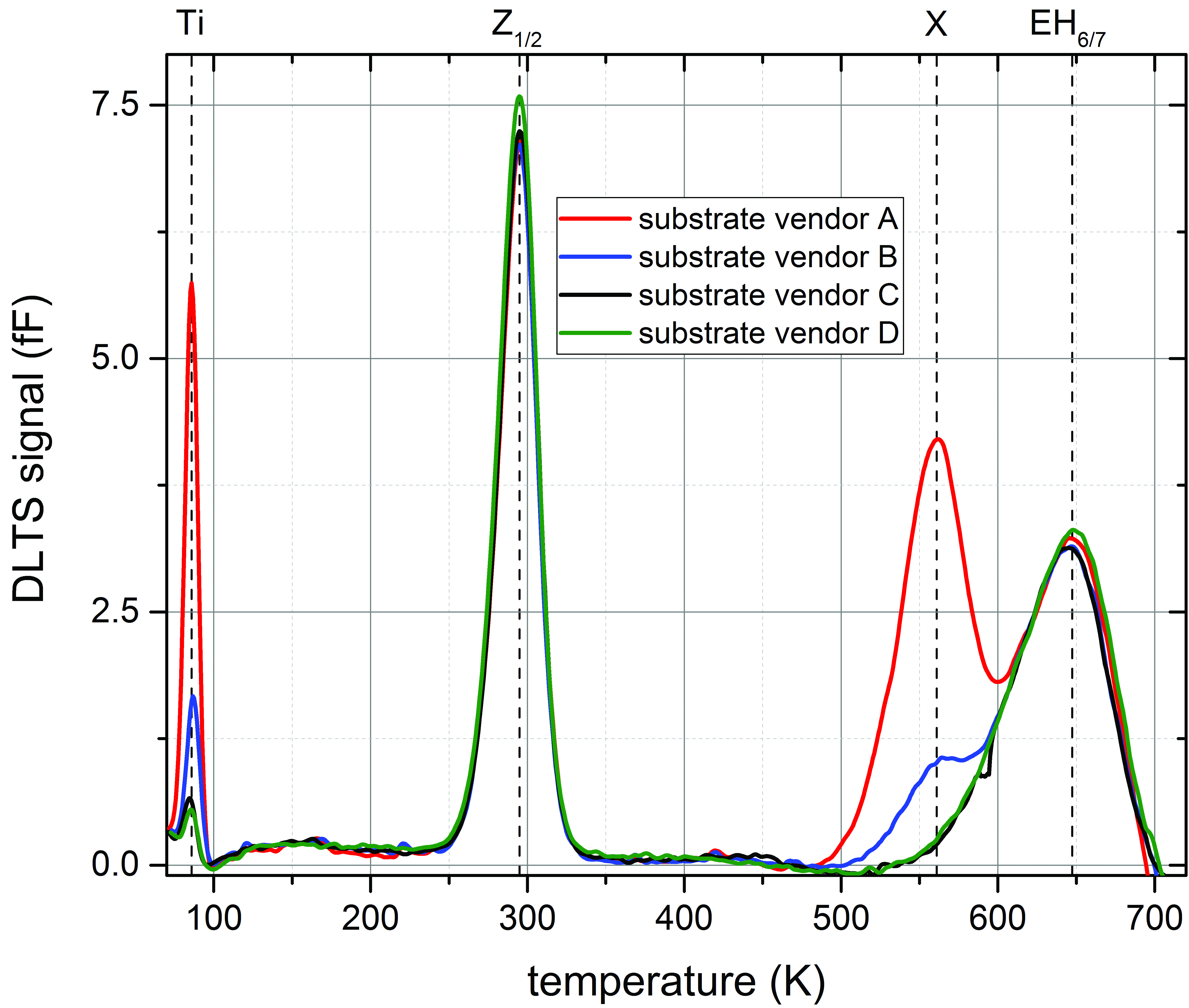
Figure 3. Deep-level transient spectroscopy has been used to probe epilayers grown on substrates from different vendors under identical epigrowth conditions. All the epilayers contain the titanium (Ti) defect and carbon vacancies (represented by Z1/2 and EH6/7). The X defect occurs only in epilayers grown on substrates from vendors A and B.
Point defectsWhen a process engineer dials in the growth temperature, gas flows and pressures, as well as influencing the impact of extended defects, their choices determine the doping concentration and thickness of the epilayers, as well as homogeneities across the wafer.
Using a modern reactor, the Aixtron G5WW, we can produce epilayers with very good doping homogeneities and a wafer-to-wafer reproducibility of less than ± 6 percent. Even more impressive results, however, are realised with Aixtron’s AutoSat technology. On 150 mm wafers, this addition reduces the wafer-to-wafer temperature uniformity from ± 3K to just ± 0.5 K. This drops the wafer-to-wafer doping deviation to less than ± 3 percent, which is an excellent result for an 8 x 150 mm production reactor.
The extremely homogeneous, reproducible temperature distribution that occurs in our epitaxial growth chamber enables some of the intrinsic point defects in the epilayers to be controlled very well, as they are generated thermodynamically. Take, for example, the carbon vacancy. It exerts the greatest influence on the carrier lifetime in n-type epilayers, and its abundance is determined by two factors: the extent of carbon excess, and the temperature during epitaxial growth.
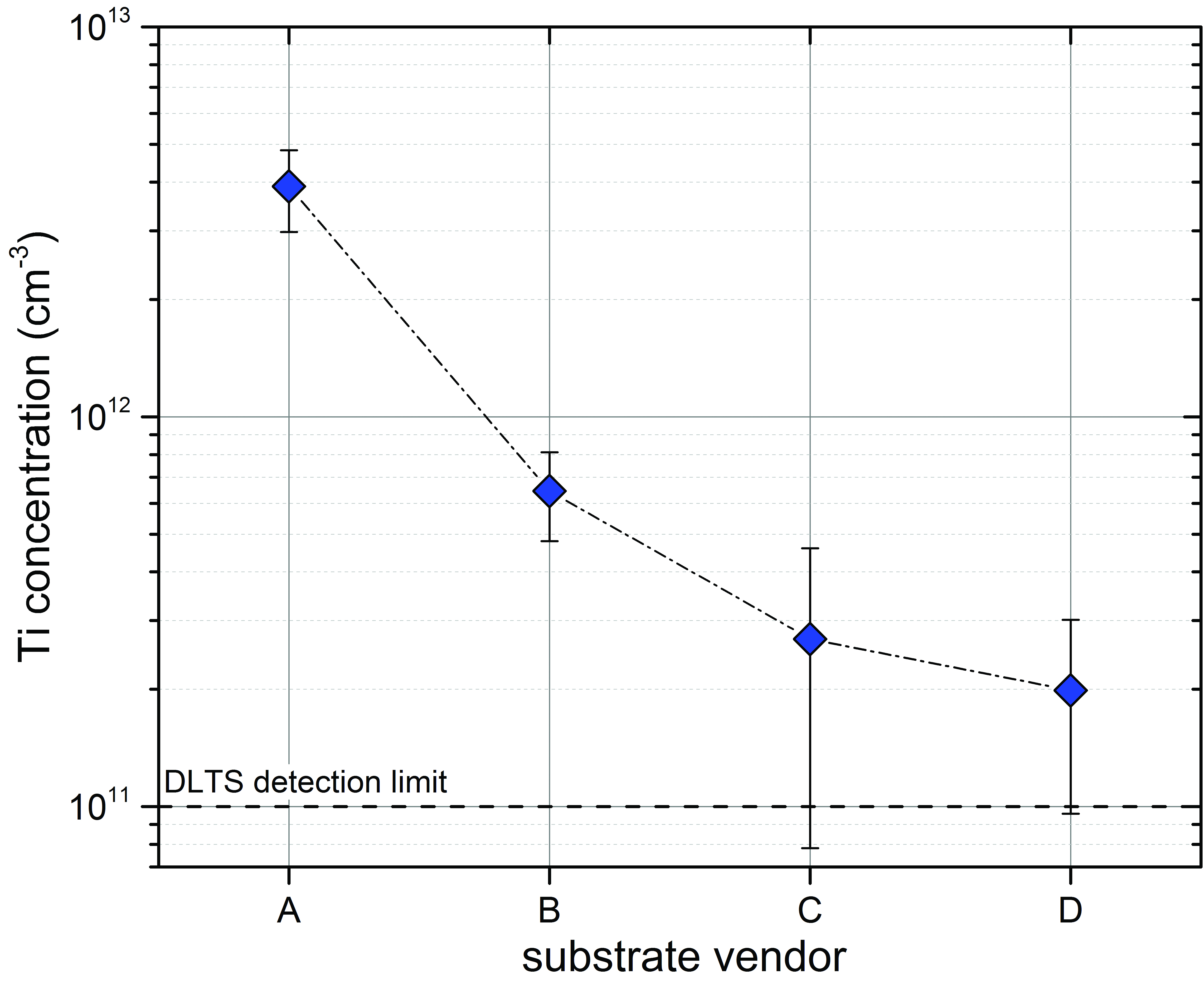
Figure 4. Data obtained from deep-level transient spectroscopy of epitaxial wafers from four growth runs shows that the titanium concentration at the top of the epilayers depends on the vendors of the substrates. Data points represent mean values, while error bars define the minimum and maximum values.
To gain insight into the point defects in n-type epilayers, we have investigated epilayers grown under identical conditions, on substrates from four different vendors. We probe all these layers, grown under conditions that ensure the same temperature, carbon-to-silicon ratio, and doping concentration, using deep-level transient spectroscopy. This technique uncovers four distinct peaks, including two associated with a carbon vacancy.For the carbon vacancy known as Z1/2, the concentration is very reproducible (see Figure 3). It is independent of the substrate used and has a level of 5 x 1012 cm-3. Other groups have also studied this vacancy, and their reports indicate that our level is very competitive. Note that we have found that the concentration of the carbon vacancy can be controlled by epitaxial growth conditions.
The titanium defect is present in all epilayers grown under identical growth conditions, but its concentration varies by a factor of 25, from 2 x 1011 cm-3 to 5 x 1012 cm-3 (see Figure 4). Its defect level is governed by the make of the substrate.
We have also studied the influence of epigrowth conditions, such as the carbon-to-silicon ratio and the temperature, on the concentration of titanium in epilayers grown on substrates supplied by one vendor. This investigation reveals that the levels of titanium are not related to the conditions during the epigrowth process or the reactor hardware. We are still investigating the mechanism for the transfer of titanium from the substrate to the epilayer.
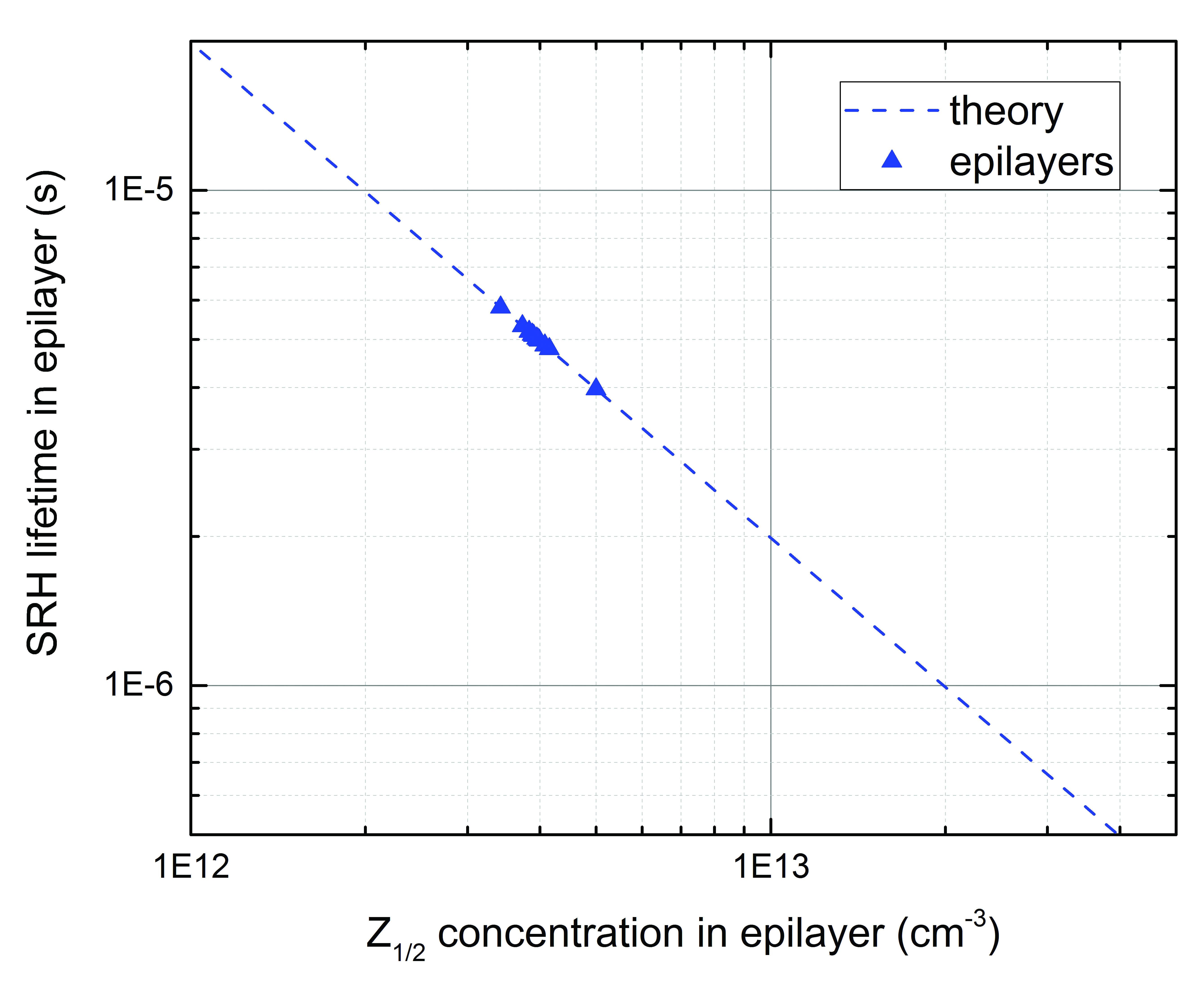
Figure 5. The Shockley-Read-Hall (SRH) lifetime as a function of the carbon vacancy concentration, calculated for microwave-detected photoconductivity decay measurement conditions (line) and individual epilayers. The Z1/2 concentration obtained from deep-level transient spectroscopy provides values used for the carbon vacancy concentration.
Deep-level transient spectroscopy also uncovered a defect that is found only in the epilayers grown on substrates provided by two of the four vendors. We are yet to determine the nature and origin of this defect, labelled X, but we plan further investigations.Carrier lifetimes
Another insight provided by deep level transient spectroscopy is that the concentration of all point defects in the n-type epilayers is, compared to the typical doping, lower by two-to-three orders of magnitude. This verifies the high quality associated with the epitaxial growth processes and the hardware.
Point defects influence the carrier lifetime in the epilayers, and can ultimately govern device performance. For example, the carbon vacancy is a known lifetime killer, and its impact on the carrier lifetime can be predicted with Shockley-Read-Hall statistics. With typical growth conditions, the concentration of the carbon vacancy varies from
1 x 1012 cm-3 to 3 x 1013 cm-3 — depending on the growth temperature and the carbon supply – and this produces variations in the carrier lifetimes from longer than 10 µs to less than 1 µs (see Figure 5). For our epilayers, the lifetime is about 5 µs, a competitive value.
The most common method for determining carrier lifetime is the microwave-detected photoconductivity decay. This method yields a value for the lifetime that depends on the Shockley-Read-Hall lifetime of the epilayer itself, but also contains contributions related to surface recombination and interface effects between the epilayer and the substrate. The value for this effective lifetime is always less than that for the Shockley-Read-Hall lifetime of the epilayer.
We have measured the carrier lifetimes on 16 epiwafers. These are taken from four runs, each containing one substrate from each of the four vendors. The results show significant differences in lifetime, dependent on the source of the substrate (see Figure 6). We are still to uncover the reason for this.
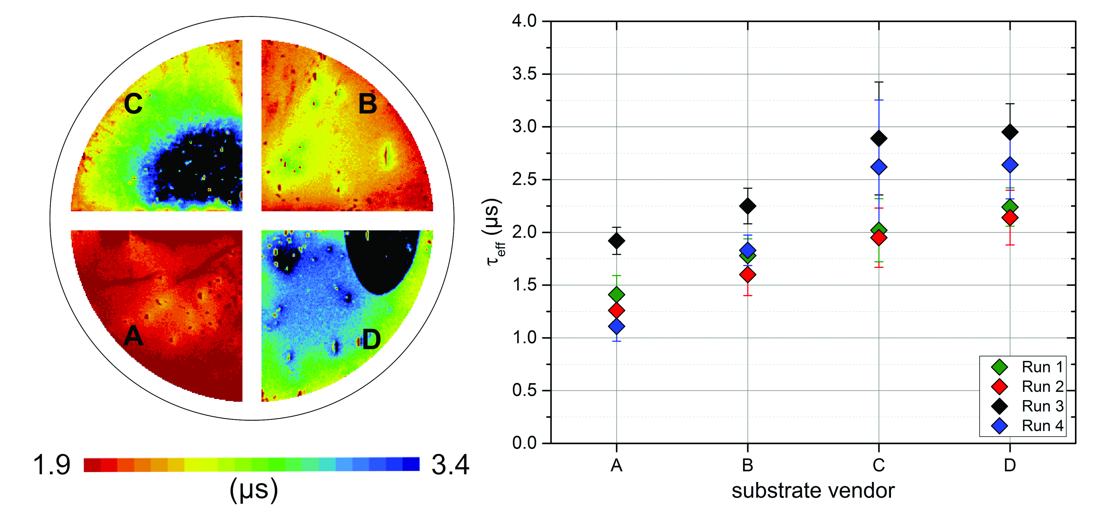
Figure 6. Effective lifetimes of 65 µm-thick, low n-doped epilayers obtained from microwave-detected photoconductivity decay. Note in wafer quarter ‘D’ the presence of extended defects as small regions with a lower lifetime and the wafer facet. Left: exemplary set of wafer quarters. Right: Effective lifetimes of 16 wafer quarters from four epigrowth runs.
Our efforts show that today’s multi-wafer reactors are capable of providing excellent homogeneities and reproducibility with regard to temperature, epiwafer thickness and doping uniformity. This enables engineers to control intrinsic point defects, such as the carbon vacancy. However, the control of some extended defects, or some influences on the effective lifetime are governed by the substrate.Fraunhofer IISB is Germany’s leading institute for applied research and development of SiC technology. Working with international partners for more than 20 years, IISB offers internationally recognized expertise in terms of SiC services and contract research – starting from materials development and characterization, and on to device manufacturing, module assembly and power electronic systems. IISB operates the π-Fab, a prototyping service which comprises a continuous silicon CMOS and SiC process line in an industry-compatible environment.
Recently, IISB and Aixtron SE have been co-operating closely in the field of SiC epitaxy – running a demonstration lab with two Aixtron G5WW reactors and IISB’s sophisticated material characterization. IISB is able to provide a fast feedback loop regarding the epilayer thickness, doping, and defect concentrations (next generation Intego ultra-violet photoluminescence imaging and surface inspection), which is one of the key factors for a successful development of epigrowth processes and hardware. IISB recently started a strategic partnership with Rigaku for beyond state-of-the-art X-ray topography of semiconductor wafers.
Birgit Kallinger is a senior scientist in the materials department of Fraunhofer IISB with about 15 years practical experience in SiC epitaxy and material characterization. She studied comprehensively SiC epitaxial growth and its impact on extended defects, mainly dislocations and stacking faults, in epilayers. In recent years, the focus of her work moved on to the impact of epigrowth parameters on point defects and carrier lifetime. Her work has been published in many research papers and been awarded several times.
Further reading
H. M. Ayedh et al. Appl. Phys. Lett. 107 252102 (2015)
T. Kimoto et al. Phys. Stat. Sol. (B) 245 1327 (2008)
J. Erlekampf et al. Materials Science Forum 924 112 (2018)
B. Kallinger et al. J. Appl. Phys. 114 183507 (2013)


