
EVG and NSI collaborate on GaAs on silicon integration
Process platform for wafer-level integration targets RF front-end module (FEM) manufacturing
EV Group, a supplier of wafer bonding and lithography equipment, has announced that it has partnered with Ningbo Semiconductor International Corporation (NSI), a specialty semiconductor foundry based in Ningbo, China, in the development of the industry's first process technology platform for wafer-level heterogeneous integration of GaAs on silicon for use in RF front-end module (FEM) manufacturing. This marks an important milestone in the development of next-generation, high-performance, ultra-compact RF front-end chipsets that are needed for 4G and 5G smartphones and other handsets.
As part of this strategic collaborative effort, EVG provided NSI with its temporary bonding/debonding (TB/DB), permanent bonding, mask alignment lithography, and related special metrology equipment and process expertise, which NSI leveraged together with its proprietary micro wafer-level system integration (uWLSI) technology platform to produce the innovative RF FEM products for a RF front-end devices and system solution provider. NSI is a joint venture subsidiary of Semiconductor Manufacturing International Corporation (SMIC) with China IC Investment Fund, Ningbo Economic Development Zone Industrial Investment Company, Ltd. and other IC investment funds.
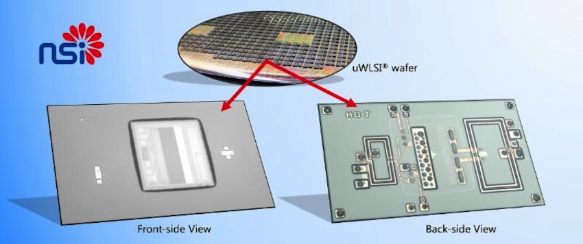
NSI's proprietary micro wafer-level system integration (uWLSI) technology.
According to Herb Huang, CEO of NSI, "High-performance, ultra-compact RF front-end microsystem components are vital to the success of the 5G wireless terminal. To support the customers and their RF front-end module products of the next generation of wireless terminals for meeting the stringent requirements of lower insertion loss, higher energy efficiency, ultra-miniaturisation, etc., it is necessary to provide more advanced wafer-level multi-chip heterogeneous integration process solutions for supporting and helping the customer meet the product standards and quickly ramp to volume production. We are pleased to have access to EV Group's leading wafer bonding technology, lithography technology and expertise in heterogeneous integration in order to facilitate the manufacturing success."
Wafer-level Heterogeneous Integration for 5G
RF FEMs include several key components, such as power amplifiers (PAs), antenna switches and filters. The high-density 3D heterogeneous integration of materials with different properties, such as GaAs and silicon, is effective in enabling improved gain, linearity and power performance for RF FEMs. At the same time, however, the migration to 5G broadband wireless technology is driving the need for wider multi-band PAs and more RF filters in the FEM, which in turn can drive up cost and footprint of the overall chipset package. Enabling heterogeneous system integration at the wafer level provides a cost-effective approach for achieving greater chipset density with minimal footprint increase.
uWLSI is a middle-end-of-line technology platform for a unique wafer fabrication process developed by NSI for enabling heterogeneous multi-die-on-wafer system integration and wafer-level system testing while eliminating the need for bumping and flip-chip processes in typical system-in-package practices. NSI developed the uWLSI technology platform to specifically address the surging need for high-density heterogeneous system integration of a variety of chipsets and microsystems through more wafer-level fabrication processing.
EVG's temporary bonding/debonding systems, like the IQ Aligner NT, play a key role in enabling the heterogeneous integration of compound semiconductors with silicon devices in a
More-than-Moore approach
EVG's TB/DB systems play a key role in enabling the heterogeneous integration of compound semiconductors with silicon devices in a More-than-Moore approach. For example, TB/DB facilitates the reliable transfer and processing of very thin compound semiconductor, silicon and mold wafers, which can be integrated into higher-density vertical packages. Likewise, EVG's mask alignment systems support wafer-level heterogeneous integration by enabling lithography patterning of carrier mounted and warped substrates, which is essential for the uWLSI process.
"NSI is at the forefront in the development of specialty semiconductors for next-generation wireless and telecommunications technologies, such as 5G," according to Swen Zhu, general manager, China, EV Group. "EVG is pleased that NSI has entrusted us once again to work with them to support their advanced manufacturing efforts -- this time on their ground-breaking development in RF FEM platforms. The expertise that we have built up as a technology and market leader in wafer bonding and lithography process solutions will play an important role in our work with this leading foundry company."
EVG will show its latest wafer bonding and lithography solutions for heterogeneous integration and other applications at SEMICON China, a leading exhibition for China's semiconductor industry, which will be held this week (March 20-22) at the Shanghai International Expo.


