Addressing production of SiC super-junction MOSFETs
A
novel ion-implantation technique improves the manufacture of SiC power
devices, including super-junction MOSFETs BY Michael Rueb FROM MI2-FACTORY
In the run-up to the turn of the millennium, a silent revolution took place in the silicon power electronics industry. Back then, the on-resistance of commercial transistors plummeted by a factor of between three and ten, thanks to the introduction of a superjunction architecture in unipolar, high-voltage devices. To create this device, a super-junction is formed by creating p-type, high-aspect-ratio columns in n-doped vertical drift zones (see Figure 1).
Today, the super-junction is a cornerstone of the silicon power industry. It features in Infineon’s CoolMOS, ST-Microelectronics MD-Mesh, Fuji’s Super J MOS series, ON Semiconductor’s Super FET and Toshiba’s DTMOS. This class of devices, which is tending to operate in the 500 V to 900 V range, is serving in switched-mode power supplies in phones, laptops, computers and even server farms. They are a invisible, integral part of our daily lives.
One of the attributes of the super-junction transistor, compared with conventional devices, is a higher doping concentration in the n-doped vertical electron conducting path. Blocking capability of the device is maintained by the p-columns, which provide local charge compensation, thereby ensuring that the global electric field is low. Thanks to this,
super-junction transistors provide an ultra-low ohmic switch with a high blocking capability. That’s great from the perspective of a chipmaker, as they can manufacture chips that are smaller – and thus cheaper – for a given on-state resistance. What’s more, these chips can fit into smaller packages.
Recently, sales of silicon power devices have faced ever-stronger competition from those based on SiC. This rival is setting a new benchmark for the efficiency of high-voltage diodes and transistors, which are being deployed in solar panels, wind turbines and electric cars. However, SiC chips are costly, so they need to improve their bang-per-buck.

Figure 1. A cross-section of a vertical silicon super-junction device.
Following in silicon’s footstepsA great way to do this is to bring to market SiC super-junction devices. This would lead to a step-change in on-resistance, and propel energy efficiency to a new high, particularly at the highest blocking voltages of 1.7 kV or more. These attributes would allow products to serve in the likes of solid-state transformers and highly efficient energy-transmission systems in high-speed trains.
Note that a related device, the SiC IGBT, is not up to this task: it suffers from a high threshold voltage – it is typically 2.7 V – and bipolar degradation of the material is an issue. Although the latter problem can be overcome, the most common solution so far is a very costly selection of the seed material and a significantly thicker epitaxial layer, leading to additional cost.
SiC super-junction devices also promise to lower the price of this wide bandgap technology, as chips can be smaller, and thus cheaper. Note that as the nominal breakdown voltage rises, the difference in drift-layer on-resistance between the super-junction design and that of the conventional, unipolar device grows, offering the potential for a greater reduction in chip size (see Figure 2).
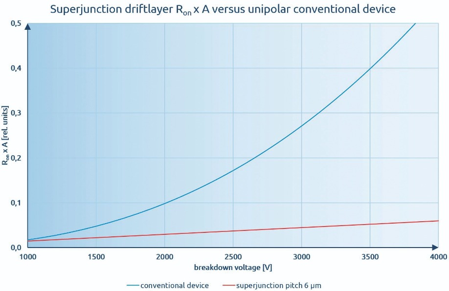
Figure 2. Drift layer on-resistance for conventional and super-junction SiC-power MOS, according to the theory described in Jpn. Patent 9701201.1
Arguably, the biggest challenge associated with the commercialisation of the SiC MOSFET is the development of suitable, high-volume processes for the manufacture of these transistors. It is not possible to simply adopt the techniques used for making silicon superjunction MOSFETs, due to significant differences between the two materials.For silicon super-junction devices, manufacture tends to involve a multi-epitaxial approach. It begins by ion implanting p- and n- areas side-by-side in an undoped epitaxial layer to define the p-type pillars. Another epi layer is deposited on top, before the implanting process is repeated. Carrying out these steps up to five-to-ten times creates ohmic p- and n-pillars, which are then subjected to a high-temperature diffusion process (see Figure 3).
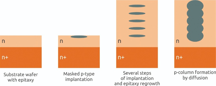
Figure 3. The manufacture of silicon super-junction devices includes a multi-epitaxy manufacturing step.
With SiC, this approach is not an option. That’s because conventional dopants, such as aluminium and nitrogen, have extremely low diffusion coefficients. This means that it is infeasible to diffuse over distances of 3-5 µm, which are required in SiC super-junction designs.Whatever approach is used has to ensure charge-balancing in the device – and so must realise highly precise doping. That rules out technologies like p-doped epi trench filling, because the doping accuracy in the high-volume production of SiC epitaxial layers is rarely better than between +/- 10 percent and +/-20 percent.
The good news is that there is a solution that is applicable to high-volume production: ion implantation, but without diffusion. We are pioneering a form of this at mi2-factory in Jena, Germany. Our technology is capable of producing deep custom-tailored dopant profiles, and while its application to semiconductor manufacturing is new, in a slightly modified flavour it has been successfully applied in heavy-ion cancer therapy for many years.
Our approach differs from the conventional one, whereby monoenergetic ions are ‘shot’ into a pre-defined depth region known as the projected range. In that case, for a given substrate and ion combination, the projected range is just defined by the ion energy. A single shot creates a gaussian peak of implanted ions. However, it is possible to form extended profiles by creating a sequence of many gaussian profiles, each originating from a different implant energy (see Figure 4).
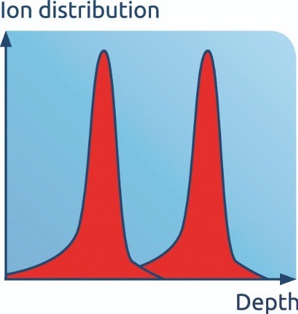
Figure 4.Two ion implantations with different energies result in essentially gaussian peaks.
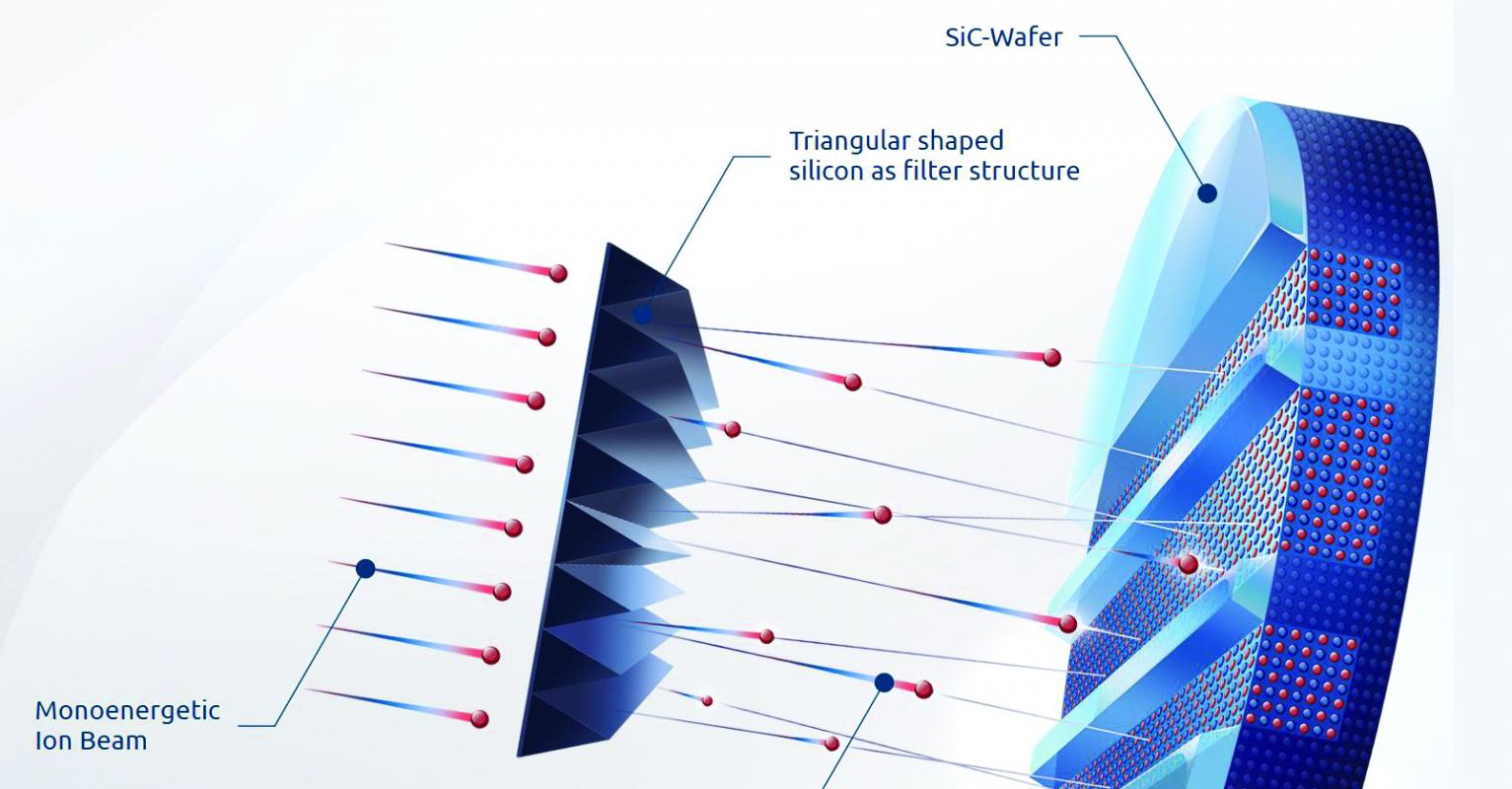
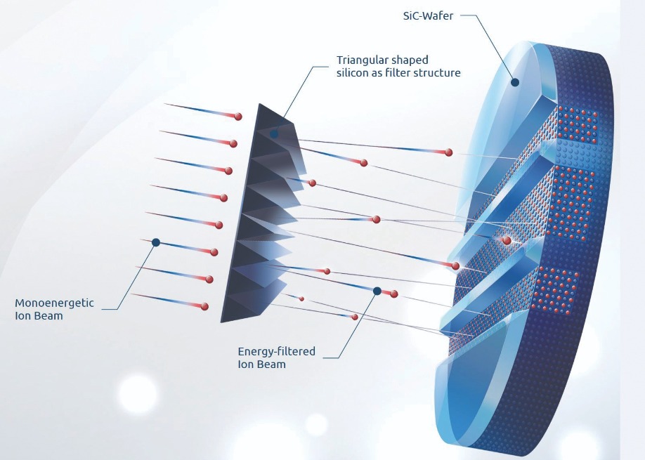
Unfortunately, extended profiles require many shots. Simulations suggest that an extended depth range of a few micrometres requires a sequence between 25 and 50 individual implants with differing energies. That’s expensive, complicated and error-prone.We advocate a far simpler approach: one shot, one ion energy and a very special filter. Known as energy filter for ion implantation, our technique involves the use of a micropatterned membrane, which converts a monoenergetic ion beam into a continuum of ion implant energies (see Figure 5). With the membrane in the path, ions are ‘shot’ not only into one depth, but simultaneously into all depths, where maximum depth is defined by the primary ion energy. With this approach, continuous depth profiles are accomplished in a very straight forward manner (see Figure 6).
Armed with our technology, high-volume manufacture of SiC super-junction transistors is possible. Our approach eliminates the need for diffusion, replacing this with a technique that delivers an extremely high level of precision. Production costs are low – just one step is required for ion implanting, with a process that is capable of both aluminium p-type doping and nitrogen n-type doping.

Figure 5. The energy filter for ion implantation pioneered by mi2 factory. The energy of primary ions is modified according to the path length individual ions have to travel through the filter membrane. The long path – through peak – leads to a high loss of energy, while the short path – through a valley – leads to a low loss of energy.
One of the primary limitations of our approach is the limited availability of mega-electron ion beams for SiC wafer manufacturing. To address this we offer SiC chip manufacturing customers a loop process option. This serves those in pilot production, and those manufacturing quantities up to medium-volume production – that is, several hundred wafers per month. For higher volumes, we recommend that fabs install industrial tandetron implanters. Further down the line, we plan to refine our technology so that it is compatible with much simpler ion-implantation equipment, rather than just today’s industrially applied electrostatic tandetrons.Although the membranes for our energy filter for ion-implantation technology are consumables, that does not prevent them from supporting stable, reliable processing. Depending on the ion dose, as many as one hundred 6-inch wafers may be implanted with just a single membrane. Given the very low membrane cost per implant, chip costs generally fall when using our technology, due to benefits that include a reduction in device dimensions associated with the super-junction design.
While our ion-implantation technique may make its case most strongly for the super-junction transistor, it also has a role to play in improving the performance of other SiC power devices, via improvements in doping accuracy (see Figure 7).
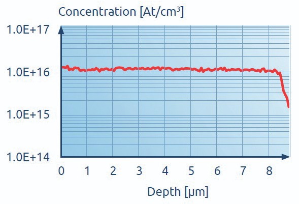
Figure 6. Nitrogen depth profile for 1200 V SiC devices.
For example, 600 V and 1200 V SiC diodes can benefit from our technology. In these devices, the drop in forward voltage is primarily determined by drift layer doping level and thickness – and optimising these two characteristics is governed by the available epi processing technology. For instance, to head off the impact of unintentional low doping levels that result from process variations, SiC diodes are generally designed larger than they would be if optimum processing conditions were available. By switching from in-situ doping during epi deposition to our superior energy filter for ion-implantation technology, we estimate that it may be possible to shrink the area of the 1200 V device by about 20 percent.This claim for a reduced chip size is supported by work that we carried out several years ago. Back in 2014, in collaboration with an industry partner, we took part in an R&D project to investigate the impact of doping precision. During this programme, we compared the variations in key characteristics of 600 V merged p-i-n Schottky diodes from regular production with those formed with our ion-implantation technology. We found far narrower parameter distributions for differential resistance, blocking voltage and leakage current, highlighting the potential of our energy filter for ion-implantation technology to reduce chip sizes (see Figure 8).

Figure 7.
The energy filter for ion-implantation technology developed by mi2
factory can be used for making diodes and transistors.
Today, our technology is well-placed to provide the essentially homogenous doping profiles that are needed for diodes and super-junctions. In future, the design of these devices is tipped to evolve, with the introduction of graded drift-layer doping profiles that will propel efficiency to a new level. We intend to support this, having just started to develop an advanced form of our technology that will be capable of delivering more complex doping profiles.
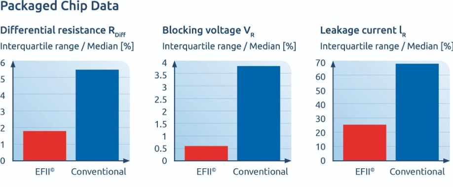
Figure 8. Results from an early R&D project with a chipmaking industrial partner highlight the reduction in the spread of key attributes for diodes.
To support this work, and ultimately our customers, we have developed a software tool that is capable of simulating all types of filter-substrate constellation. This includes masked substrates (see Figure 9).We are confident that interest in our technology will grow. The SiC super-junction is destined to deliver a hike in power-transistor efficiency, and our energy filter for ion-implantation technology is a key enabling technology for the production of these devices. Other diodes and transistors will also benefit from our approach to doping, with the greater accuracy provided by our technology enabling a trimming of dimensions, leading to significant cost savings.
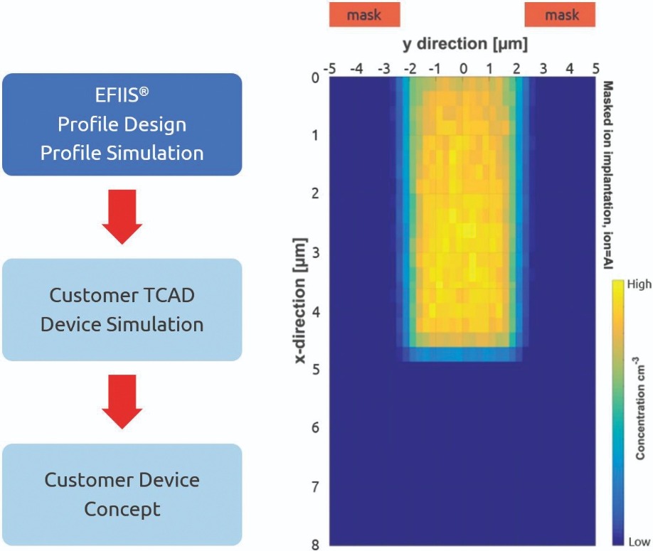
Figure 9. Left: The approach that mi2 factory takes for supporting customer device design with its energy filter for ion-implantation. Right: A 5 µm-deep p-column created in SiC using an energy filter for ion-implantation.
T. Fujihira et al., “Semiconductor device with alternating conductivity type layer and method of manufacturing the same,” Jpn. Patent 9701201.1 (1997)
G. Deboy et al. IEDM 683 (1998)
F.Udrea et al. IEEE Trans. Electron Devices 64 713 (2017)
R. Rupp et al. Materials Science Forum 858 531 (2016)
S. Agostinelli et al. Nucl. Instrum. Methods Phys. Res 506 250 (2003)


