

Graphene brightens deep UV LEDs
Multi-layer graphene quashes defects in AlN, leading to a hike in LED efficiency

Researchers from Beijing have cranked up the output power of deep UV LEDs by inserting a layer of graphene between the substrate and the epilayers.
The team’s efforts could aid the development of more powerful deep UV sources for the likes of sterilisation, polymer curing, biochemical detection and speciality lighting. Today, the use of LED in these applications is held back by a low internal quantum efficiency – it is typically below 10 percent.
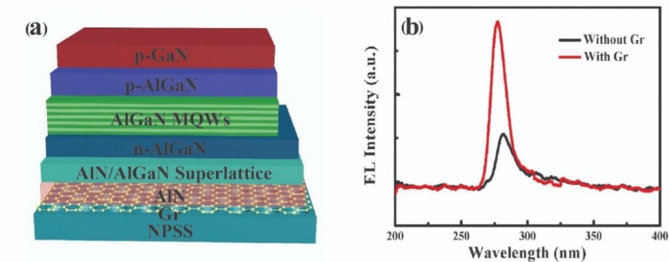
Improvements in the efficiency and brightness of the UV LEDs produced by the team from Beijing resulted from the first growth of high-quality AlN films on nano-patterned sapphire substrates by graphene-assisted quasi van de Waals epitaxy.
Using this approach, coalesce occured in films of AlN as thin as just 1 µm. This is one-third of the thickness for the standard method, involving the growth of AlN films on patterned sapphire. Substantial savings result, both in terms of growth time and material costs.
To understand the benefits of their approach, the team undertook first-principles calculations to determine energy migration barriers for aluminium on sapphire and on graphene. On the former it is 1.02 eV, while on the latter it is smaller by more than an order of magnitude, explaining why a layer of graphene promotes lateral migration of aluminium atoms.
Enhanced migration is a tremendous virtue, because it encourages two-dimensional growth. “That not only causes rapid lateral coalescence of AlN on the nano-patterned sapphire surface, but also reduces dislocation density and strain release in the AlN epitaxial layer,” explains team spokesman Tongbo Wei from the Institute of Semiconductors, Chinese Academy of Sciences.
In turn, trimming the dislocation density and reducing the strain improves the quality of the active region, leading to a higher internal quantum efficiency and brighter LEDs.
The team used imprint lithography and etching to create nano-patterned sapphire, featuring a hexagonal array of 400 nm deep cones, with a period of 1 µm.
After loading the patterned substrate into an MOCVD reactor, the researchers added graphene layers using quasi van de Waals epitaxy. Then, to increase the chemical reactivity of the graphene layer – epitaxial growth of AlN on graphene is known to be difficult – the researchers turned to nitrogen active-ion etching plasma treatment to introduce defects into the film.
To evaluate the impact of this process, the team produced two samples: one had an AlN film grown on a graphene layer on nano-patterned sapphire, while the other did not contain the graphene.
Scanning electron microscopy revealed that with the addition of graphene, the irregular AlN islands disappeared – they were replaced by a featureless, flat film. This form of microscopy also showed that with the graphene layer, AlN can completely coalescence when the film thickness is less than 1 µm. In comparison, for AlN on nano-patterned sapphire, a 2.4 µm-thick film of AlN is required for complete coalescence.
Raman spectroscopy revealed reduced strain with the addition of graphene. Strain fell from 0.87 GPa to 0.25 GPa. To evaluate the dislocation density in the AlN, the team scrutinised this epilayer with bright-field, cross-sectional transmission electron microscopy.
This showed that the density of dislocations is 5.5 x 109 cm-2 near the interface, but just 1.5 x 109 cm-2 on the surface of a 1.5 µm-thick film.
The superior AlN led to better LED performance. 280 nm-emitting devices that included the graphene film produced an electroluminscence peak 2.6 times stronger than conventional variants.
One of the goals for the team is to further investigate the effect of graphene on the properties of the LED.
“More importantly, we will try to separate the AlN epilayer from sapphire with the help of the weak van der Waals forces between the multi-layer graphene, to obtain flexible LEDs,” says Wei. “Quasi van de Waals epitaxy has great potential to fabricate flexible LEDs, taking the place of laser lift-off.”
Reference
H. Chang et al. Appl. Phys Lett. 114 091107 (2019)
Multi-layer graphene improves epilayer quality, leading to more-efficient deep UV LEDs.