
Adding indium Ups the power of the UV LED

The addition of an indium-based underlayer traps surface defects, leading to a hike in internal quantum efficiency
Near-ultra-violet LEDs are plagued by a low external quantum efficiency that hampers development of white LEDs based on red, green and blue phosphors.
But this could all change, thanks to the work of researchers from EPFL and the Swiss Federal Laboratories for Materials Science and Technology. This partnership has shown that inserting an InAlN underlayer beneath a near-UV LED delivers a hike in internal quantum efficiency from below 10 percent to well over 60 percent.
Speaking on behalf of the team, Camille Haller from EPFL told Compound Semiconductor that indium is the key ingredient in the interlayer. The researchers think that this traps surface defects, preventing them from being incorporated in the active region, where they would lead to the creation of non-radiative recombination centres.
As yet, there is no theoretical support for this conjecture. “The role of the underlayer is highly debated, but we have already ruled out the impact of strain, the electric field, and screening of dislocations due to V-pit formation,” says Haller.
What is abundantly clear, however, is that the indium-containing interlayers are beneficial in nitride-based LEDs. “The striking feature is that all commercial blue LEDs feature an InGaN underlayer – bulk or superlattice – whatever the substrate is,” argues Haller.
Along with her co-workers, she has proven the benefit of InAlN underlayers in near-UV LEDs by making devices with and without this ternary, and comparing their performance. Samples were made by loading sapphire substrates into an Aixtron 200/4 RF-S MOCVD reactor and growing various epistructures, which all begin with a 2 µm-thick GaN buffer layer.
On top of this a 5 nm-thick layer of silicon-doped GaN is added in the control sample. Of the two variants, one features a 45 nm-thick layer of silicon-doped In0.17Al0.83N, followed by a 5 nm-thick layer of silicon-doped GaN; and the other has a superlattice, containing 24 interleaving pairs of 2.1 nm thick silicon-doped In0.17Al0.83N and 1.75 nm-thick silicon-doped GaN, followed by a 5 nm-thick layer of heavily silicon-doped GaN. Added on top of all three samples is an LED epistructure that features an active region with a single, 2.7 nm-thick In0.09Ga0.81N quantum well and a 20 nm-thick magnesium-doped Al0.2Ga0.8N electron-blocking layer.
All three types of epiwafer were processed into 300 µm by 300 µm LEDs, formed with a titanium and gold stack for the n-type contact and a combination of palladium and gold for the p-type contact.
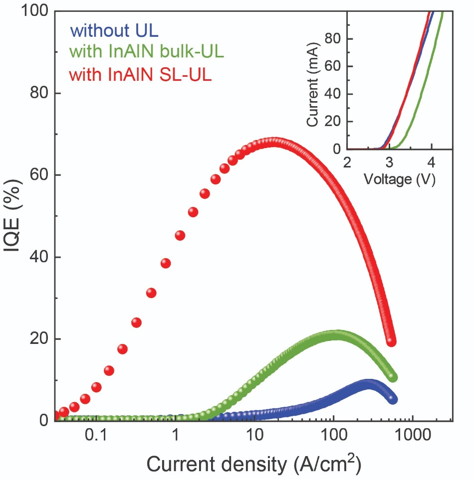
Measurements of the internal quantum efficiency at a range of drive currents revealed a peak at 9 percent for the LED without the interlayer, and a maximum value of 21 percent for the chip with the bulk InAlN interlayer (see Figure). This moderate gain in performance is attributed to imperfections in the AlInN layer, which might be hampered by V-type pits.
One drawback of the bulk InAlN layer is that it leads to an increase in turn-on voltage – a bias of 3.26 V is required for a 20 mA current, compared with just 3.16 V for the control (see inset to figure). Polarisation mismatch at the second InAlN/GaN interface is thought to be the culprit, creating an electrostatic barrier.
The barrier is addressed with very high doping at the interface. This is employed in the LED with the superlattice – it has a smooth surface, high structural quality, and enables an internal quantum efficiency of 68 percent.
Haller says that the team will continue to work on understanding surface defects. Efforts will focus on comprehending the creation of these imperfections, and identifying them.
Reference
C. Haller et al. Appl. Phys. Express 12 034002 (2019)
Placing an superlattice of InAlN and GaN underneath a UV LED boosts internal quantum efficiency without compromising the turn-on voltage


