
Magnesium doping varies with the plane of GaN

Cathodoluminescence reveals that sidewalls have a significantly lower magnesium content than standard GaN epilayers
Researchers from Arizona State University are claiming to have broken new ground by being the first to image lateral variations of magnesium doping efficiency in mesa structures.
This finding has implications for vertical GaN power devices, which are preferred for high-voltage, high-power applications, thanks to their high-voltage and high-power handling capability, good thermal management and compact design.
Fabrication of these devices involves the etching of epiwafers, followed by GaN re-growth on different planes. The magnesium doping in these devices must be uniform and high enough to pinch off the channel without any bias, and ultimately ensure normally-off operation. Based on this latest work, uniformity is challenging, given that different planes have different magnesium concentrations.
The researchers uncovered variations in magnesium doping concentration with cathodoluminescence (CL) measurements. Secondary ion mass spectroscopy (SIMS) could not have revealed this lack of uniformity, due to insufficient spatial resolution.
According to spokesman for the team, Fernando Ponce, the biggest challenge with their cathodoluminescence measurements is to correlate the luminescent characteristics with the magnesium doping in the control samples.
To carry out their investigation, the team used MOCVD to produce four different samples. The first is formed by growing a 4 µm-thick unintentionally doped layer of GaN, before using photolithography and chlorine-based inductively coupled plasma etching to produce a mesa structure, and then adding a 0.3 µm-thick unintentionally doped layer of GaN, followed by 1.65 µm-thick p-type GaN. The other three samples were produced by growing, on sapphire, a 1 µm-thick layer of n-type GaN, followed by a 1.65 µm-thick layer of p-type GaN. The difference between these samples is the flow rate for the source of magnesium, Cp2Mg – values of 50, 100 and 200 sccm created samples with differing p-type doping concentrations.
All four samples were annealed at 800 °C for 10 minutes to activate the magnesium doping. After this, the researchers used SIMS to determine the magnesium concentrations in the three planar samples.
Cross-sectional CL imaging and spectroscopy of the mesa structure revealed peaks at 2.9 eV, 3.25 eV and 3.4 eV, with relative intensity varying with location. These three peaks, which are seen in CL spectra from all three planar samples, have been observed by other groups. The peak at 3.4 eV has been attributed to near-band-edge excitonic transitions, while that at 3.25 eV stems from shallow-donor to magnesium-acceptor transitions, and that at 2.9 eV is associated with deep-donor to magnesium acceptor transitions.
By comparing CL spectra from the mesa structure to the spectra from the planar samples, the researchers concluded that the magnesium concentration in the upper mesa, the bottom of the lower mesa, and the centre of the lower mesa away from the sidewalls is about 3.1 x 1019 cm-3. That’s because the spectra resembles that from the sample produced with a Cp2Mg flow rate of 100 sccm. For the sidewall and the top of the lower mesa, the spectra is similar to that produced by the sample with a Cp2Mg flow rate of 50 sccm – it has a magnesium concentration of 1.3 x 1019 cm-3.
Reference
H. Liu et al. Appl. Phys. Lett. 114 082102 (2019)
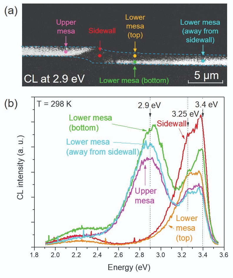
Cross-sectional optical properties of the mesa structure. Monochromatic cathodoluminescence mapping at 2.9 eV. (b) Spot-mode cathodoluminescence spectra in different regions in the p-GaN layer, as indicated by arrows in (a).


