
Another step towards silicon optoelectronic Integration
Chinese team demonstrates progress in silicon electro-optic modulator performance for future optoelectronic interconnects
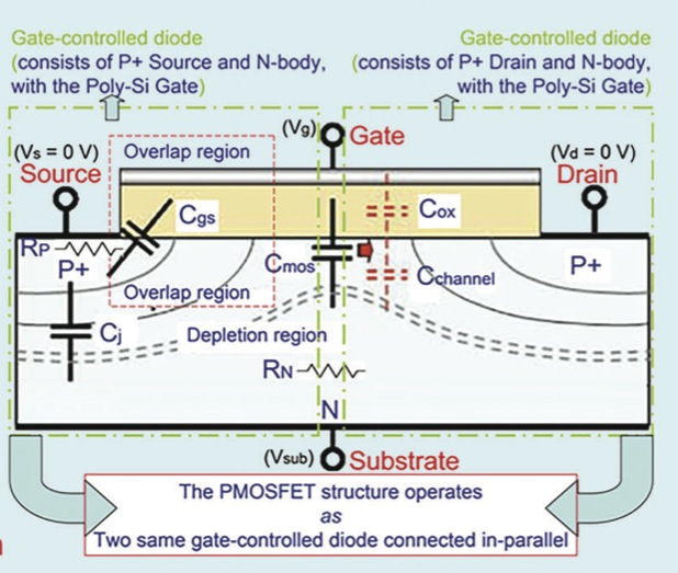
In a recent paper in Phys. Status Solidi A, Chinese researchers have demonstrated light emission from a silicon p‐channel MOSFET with a 6μm effective gate length that is operated as a three‐terminal gate‐controlled LED.
Using a photon‐emission microscope with a detector responsive to the range of 200–1000 nm, they measured emission spectra in the range of 400 to 900 nm which includes visible light radiation.
The team, led by Kaikai Xu at the State Key Laboratory of Electronic Thin Films and Integrated Devices in the University of Electronic Science and Technology of China, say the fabrication of the device is fully compatible with CMOS processing procedures.
Since the MOS‐like diode uses the field effect induced by the gate for modulation of the diode's space charge electric field (and hence the optical output from the LED), the modulation speed for visible and infrared bands can attain high frequencies in the GHz range.

Such high frequencies represent a significant leap in silicon electro-optic modulator performance for future optoelectronic interconnects using standard CMOS processes.
The lifetime of the MOS-capacitor LED should be controllable via the capacitor discharge time. In other words, the Si gate-controlled diode LED operates on the principle of the MOS-capacitor and not on standard p-n junctions. In contrast to the lifetime of carriers in the depletion region, the MOS-capacitor discharge time also determines the modulation in the reverse-bias silicon p-n junction with gate control.
Light generation from a Si‐LED provides a way to manufacture all‐silicon monolithically integrated optoelectronic systems composed of CMOS transistors and Si‐LEDs fabricated on the same chip.
'Silicon MOS Optoelectronic Micro‐Nano Structure Based on Reverse‐Biased PN Junction' by Kaikai Xu; Phys. Status Solidi A March 2019 https://doi.org/10.1002/pssa.201800868


