
Interband cascade lasers target the mid-infrared
Inventor of the interband cascade laser, Rui Q. Yang from the University of Oklahoma, details the progress of this powerful, efficient mid-infrared light source that combines the best assets of laser diodes and QCLs
There is a strong, ever growing demand for reliable semiconductor lasers emitting in the mid-infrared. Sources in this spectral range, which extends from 3 µm to 12 µm, are required for many applications, including environmental and chemical-warfare monitoring, gas sensing, the detection of pipe leaks and explosives, food safety, industrial process control, medical diagnostics, infrared lidar, free-space communications and infrared illumination.
Producing an efficient, compact mid-infrared semiconductor laser is far from easy, due to a combination of fundamental and technological issues. But it can be done, by pursuing less common architectures, such as interband cascade lasers (ICLs) and quantum cascade lasers (QCLs).
These cascade-based devices are needed, because the conventional diode laser struggles to operate in the mid-infrared. Its emission is determined by its bandgap (see Figure 1 (a)), and it’s impossible to reach the mid-infrared with either of the two more mature material systems, the arsenides and the phosphides. Meanwhile, narrower bandgap materials are held back by weaker bonding between their constituent atoms.
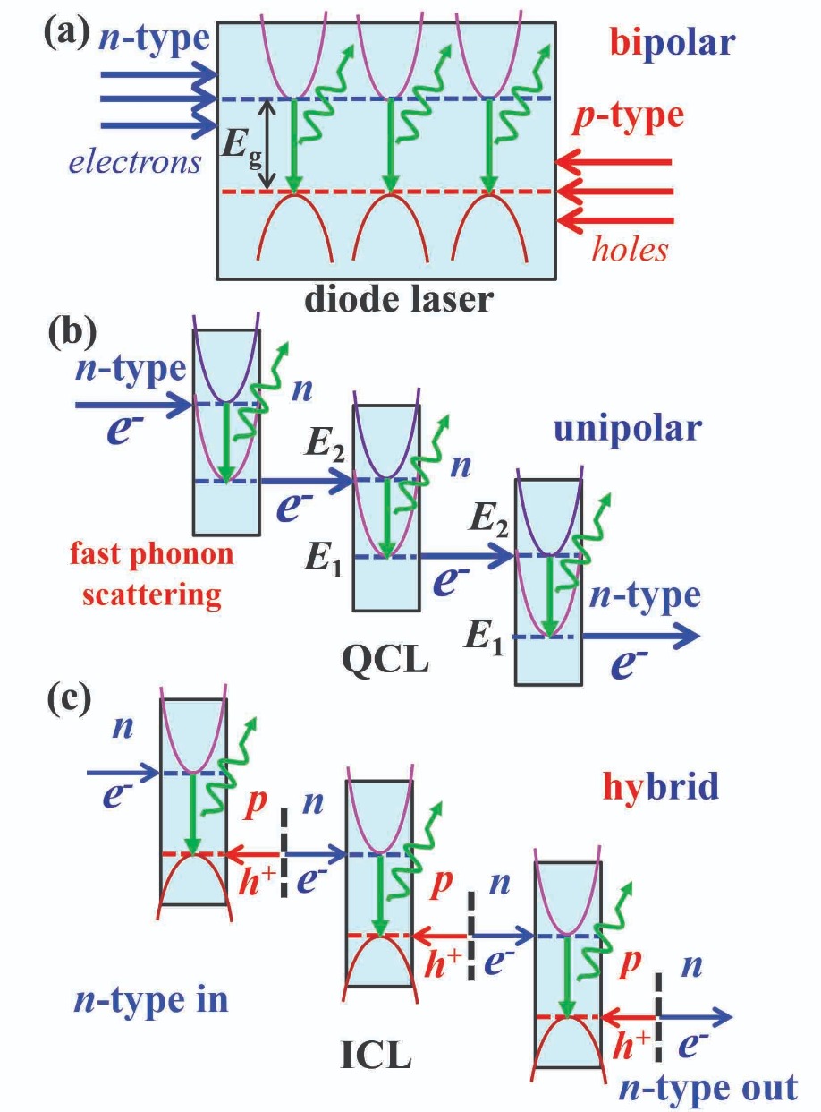
Figure 1. (a) conventional bipolar (electron and hole) diode laser; (b) unipolar intersubband QCL; (c) and an interband cascade laser (ICL) combining advantages of the first two. Note that the conduction and valence bands have opposite energy-wavevector dispersion relations, while sub-bands within the same conduction band have a similar energy-wavevector dispersion relationship.
An additional drawback of the conventional diode laser is that as the emission wavelength stretches further into the infrared, there is a hike in non-radiative loss mechanisms, such as Auger recombination, while other issues come to the fore, including inadequate electrical confinement, poor efficiency in utilising the bias voltage, a non-uniform distribution of injected carriers and increased free-carrier absorption loss. Given all these impediments, it is of no surprise that mid-infrared diode lasers, such as lead-salt lasers that are based on IV-VI materials, need to be cooled with liquid nitrogen to operate, and they produce a feeble output power while suffering from mode-instability.Despite all these difficulties, progress has been made with the conventional architecture, in the form of a type-I GaInAsSb quantum well diode laser. It can deliver room-temperature emission, but only up to wavelengths of about 3.7 µm – try to push the output further into the mid-infrared, and threshold current densities rise rapidly (see Figure 2).
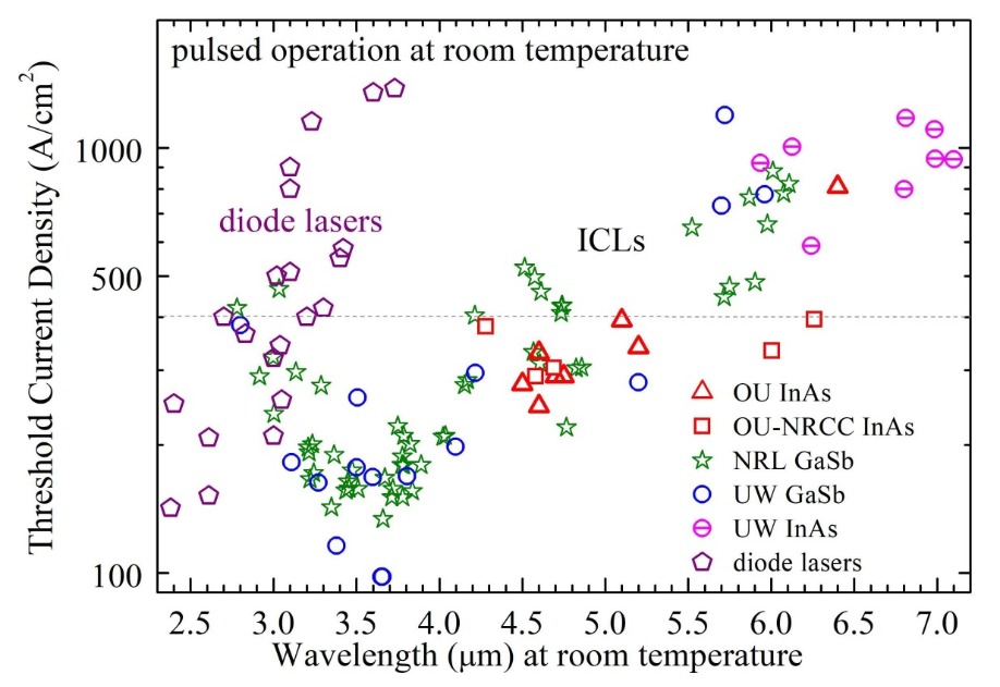
Figure 2. Pulsed threshold current density of conventional diode lasers from literature and type-II broad-area ICLs based on GaSb and InAs substrates at room temperatures (20-27 °C). ICLs were made at the Naval Research Laboratory (NRL), University of Wurzburg (UW), University of Oklahoma (OU) and National Research Council of Canada (NRCC).
Turning to the ICL tackles many of these issues. Similar to the unipolar QCL, where the wavelength of its emission is determined by its intersubband energy difference (see Figure 1(b)), high quantum efficiencies result, with every injected electron cascading through several stages connected in series, to generate multiple photons (see Figure 1(c)). As this mode of operation ensures uniform injection of electrons over every stage, the carrier concentration required for threshold is lower than that in conventional diode lasers, resulting in reduced optical and Auger losses and a lower threshold current density. This allows the laser to operate at a lower current, trimming the parasitic loss due to electrical resistance to a value below what it would be in a conventional diode laser.When it comes to design, there are also advantages associated with the ICL. Conventional bipolar diode lasers require n-type and p-type cladding regions, while ICLs just need an n-type cladding, inserted at either end of the cascade stages to transfer electrons in and out. Eradicating p-type layers is beneficial, because they tend to absorb more light than their n-type counterparts, and thus result in higher losses. Note that the interfaces between the adjacent cascade stages can be viewed as semi-metallic, in which electrons and holes are generated internally.
A significant difference between the ICL and the QCL is the light-generation process. Lasing in a QCL results from intersubband transitions, dominated by fast phonon scattering, occurring on a time scale of picoseconds or less. Meanwhile, with ICLs, photons are generated in optical transition between conduction and valence bands, in which the carrier lifetime is typically on the order of nanoseconds. This far longer carrier lifetime is a big deal – it allows the threshold current density in ICLs to be far lower than in QCLs. What’s more, population inversion can be established without using fast multi-phonon-mediated depletion, resulting in a high voltage efficiency.
The superiority of the ICL over the QCL extends to the nature of its emission. The polarized output from an ICL is transverse electric, while that from a QCL is transverse magnetic. It means that it is possible to make interband cascade VCSELs. Such a device has already been demonstrated by researchers at NRL: they have made a 3.4 µm interband cascade VCSEL operating in pulsed mode at temperatures of up to 70 °C.
So it is clear that ICLs have tremendous potential, combining the best attributes of diode lasers and QCLs. They promise to be the most efficient class of semiconductor mid-IR lasers, in terms of both power consumption and the threshold input power density.
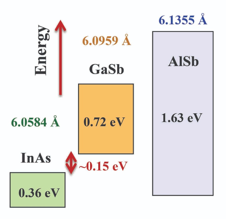
Figure 3. Bandgaps, band-edge offsets and lattice constants of InAs/GaSb/AlSb materials.
Device designICLs are constructed by taking either GaSb or InAs substrates, loading them into an MBE chamber, and growing nearly lattice-matched heterostructures from the likes of InAs, GaSb, AlSb and their related alloys (see Figure 3, illustrating the unique variety of band alignments). In this material system, the conduction-band-edge of InAs is lower in energy than the valence-band-edge of GaSb, so this pairing of materials forms a semimetal-like hetero-interface – a unique feature in type-II broken-gap heterostructures and quantum wells. Another advantage of the broken-gap alignment is that it facilitates the efficient interband tunneling needed for re-using injected electrons within the device.
In a typical type-II ICL, repeated active regions are separated by electron and hole injection regions, consisting of digitally graded InAs/AlSb and GaSb/AlSb quantum wells (see Figure 4). In each active region, containing InAs/GaInSb type-II quantum wells, optical transitions occur between the conduction states of InAs and the valence state of GaInSb, with wave-functions for the electrons and holes primarily residing in the respective layers.
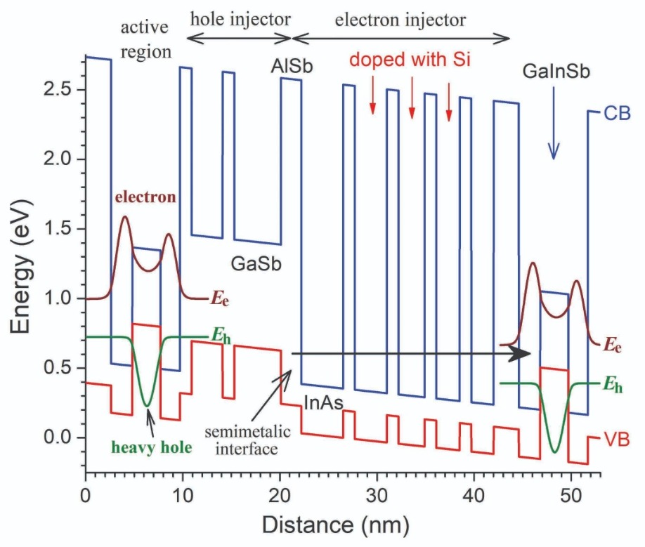
Figure 4. The layer sequence for an ICL, and conduction band (CB) and valence band (VB) edge profiles under forward bias.
To produce a high-performance ICL, engineers must ensure that the ground level for the electron in the InAs quantum well is positioned within the bandgap of GaSb. Doing this suppresses leakage current, because electrons injected into this section cannot directly tunnel out by the AlSb and GaSb layers. Instead, they undergo interband transitions to the valence state, thereby reaching the next stage.After making this transition, the electrons travel through the valence band GaSb quantum well, before undergoing interband tunnelling, to arrive in the conduction band of the electron injector in the next cascade stage. Here, they are reused for additional photon emission.
One of the merits of the InAs/AlSb/GaSb material system is its large conduction and valence-band offsets, which ensure excellent carrier confinement. With this material system, the wavelength of the emission is controlled by simply adjusting the thicknesses of the type-II InAs and GaInSb quantum wells. Without changing constituent materials, emission wavelengths can span mid-infrared wavelengths from 2.5 µm to 12 µm. And even that’s unlikely to be the longer-wavelength limit, given that type-II IC LEDs have producedelectroluminescence beyond 15 µm.
Performance milestones
Since proposing the first ICL at The 7th International Conference on Superlattices, Microstructures and Microdevices, held in Banff, Canada in 1994 – the year of demonstration of the first QCL – this class of device has come on in leaps and bounds. Now these devices combine high-performance with wide wavelength coverage, which spans 2.7 µm to 11 µm for devices based on type-II quantum wells. Milestones for the ICL include: producing room-temperature operation with low threshold current densities at wavelengths spanning 2.7 µm to beyond 6 µm (see Figure 2); CW operation at temperatures of up to 115 °C; power consumptions less than 0.1 W, at threshold at 300 K; and CW output powers exceeding 500 mW.
Today GaSb-based ICLs, which led the development of this class of laser, are relatively mature in the 3-4 µm wavelength range. Much progress has also been made with InAs-based ICLs, which mainly cover wavelengths beyond 4 µm. Note that in the 4-6 µm region, InAs- and GaSb-based ICLs have comparable threshold current densities, but beyond 6 µm, InAs-based ICLs deliver a better device performance. However, it’s important not to make any hard and fast rules. At longer wavelengths, GaSb-based and InAs-based ICLs have not been extensively investigated, and both types of laser have the potential for much improvement.
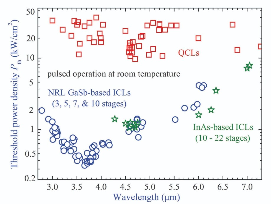
Figure 5. Threshold input power density for room temperature QCLs and ICLs.
In this spectral range performance is hampered by significant Auger recombination and free-carrier absorption loss, as well as a reduction in gain that stems from a decrease in the wavefunction overlap between electron and hole states. With these factors at play, one might expect the lasing threshold current density to increase as the lasing wavelength approaches 7 µm and beyond (as is shown in Figure 2). However, it is premature to project where the boundary is, given the relatively modest increase in threshold current density with increases in the lasing wavelength from 4.3 µm to 6.3 µm.The low threshold current densities in ICLs combine with low threshold voltages – typically between 2 V and 5 V – to produce a low threshold input power density. For emission in the 3 µm to 4 µm range, values can be as low as 0.35 kW/cm2 (see Figure 5), which is an order of magnitude below the best QCL results. This validates the superiority of ICLs as energy-efficient mid-IR laser sources. They offer this attribute over a wide spectral range – type-II IC lasers, based on both GaSb and InAs substrates, can produce energy-efficient, CW operation at room temperature and above across a spectral range spanning 2.7 µm to 6.3 µm. With energy costs and environmental concerns destined to rise in the future, these energy-efficient ICLs are well-positioned to serve in many practical applications, such as portable instruments that could include battery-powered sensors in the field and network.
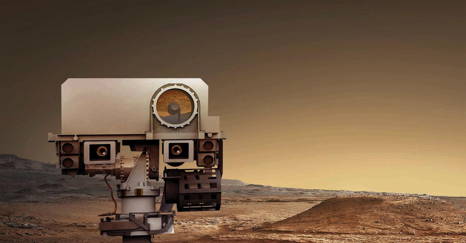
Equip the ICL with distributed feedback, and it can produce single-mode operation. This is enabling these lasers to be used for the detection of important molecules such as H2CO, CH4, C2H6, C2H4, HCl, and CO. It is this application that has allowed the ICL to hit the headlines. A flight instrument aboard NASA’s Curiosity rover, equipped with a distributed-feedback ICL, landed on Mars in August 2012 and has successfully detected methane. It is still working on Mars.
At longer wavelengths in the mid-infrared, ICLs are overshadowed by QCLs. Beyond 7 µm, QCLs are still delivering high performance at room temperature, while ICLs are yet to produce room-temperature operation. Innovation will be required to overcome this barrier, but there is hope – ICLs have exhibited threshold current densities of just 2-10 A/cm2 at 80K, with little sensitivity to the lasing wavelength over 3-10 µm. Combining these low current densities with a low threshold voltage of typically 2-5 V leads to a very low power consumption for ICL narrow-ridge lasers – it can be below 10 mW at 80K.
Such a low power consumption is a major asset in applications requiring devices with highly sensitive, low-noise detectors at long wavelengths. In such scenarios, the detectors have to be cooled to minimise noise, so a cooling platform is readily available – and if the power consumption of the ICL is less than 10 mW, that is not much of a burden on the cooling environment. In other words, it is feasible to add an efficient ICL, to create a significant energy saving. Ultimately, this could enable more applications, thanks to a reduced system size and cost.
Interband cascade bandwagon
Uses of the interband cascade structures are not limited to efficient mid-infrared lasers. This class of heterostructure can also be used to make high performance mid-infrared LEDs, as well as photodetectors and photovoltaic cells that convert mid-infrared light into electricity. Preliminary efforts have demonstrated high-performance, room-temperature IC infrared photodetectors with cut-off wavelengths spanning 3 µm to 12 µm, and promising IC thermophotovoltaic cells. These results underscore the feasibility of integrating different functional devices on the same chip – and approach that could lead to miniaturised mid-infrared modules and systems.
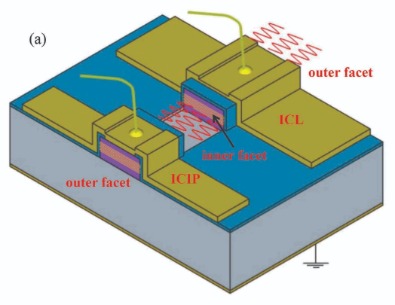
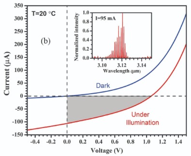
Figure 6. (a) An interband cascade laser and detector. (b) The current-voltage characteristics for the detector under dark and laser illumination. Inset shows the laser emission spectrum from the outer facet.
Our team at the University of Oklahoma is developing this type of technology. We have monolithically integrated an ICL and detector (see Figure 6). This device has an open-circuit voltage of 1.06 V, which is nearly three times the bandgap, indicating the highly effective action of cascade. Peak detectivity is 1.9×10¹⁰ Jones at 20 °C, the highest reported value for mid-infrared detectors at room temperature.This survey of interband cascade devices, and lasers in particular, shows that this technology is clearly making a transformative change to the mid-infrared landscape with much progress. The coming years are sure to witness further improvements in performance and more expansion to less explored or even new aspects such as frequency combs, highlighting the capability of this class of device for serving the mid-infra-red.
R. Q. Yang, “Interband Cascade (IC) Lasers”, Chap. 12, in Semiconductor lasers: Fundamentals and applications, edited by Baranov and E. Tournie (Woodhead Publishing, 2013)
I.Vurgaftman et al. J. Phys. D: Appl. Phys. 48 123001 (2015); Encyclopedia of Analytical Chemistry (2016)
J. Koeth et al. Proc. SPIE 10403 1040308 (2017)
S.M.S. Rassel et al. Opt. Eng. 57 011021 (2018)
W. Huang et al. Infrared Phys Technol. 96 298 (2019)
There are now three companies producing and selling ICLs: nanoplus in Germany; Thorlabs in the US; and the Swiss company Alpes Lasers, which has licensed NRL patents. In addition, several research institutions are developing ICLs, including NRL, University of Oklahoma, University of Wurzburg, National Research Council of Canada, the University of Montpellier, and Institute of Semiconductors at Chinese Academy of Sciences. In comparison, far more firms and groups are working on QCLs, partly because the antimonide-based III-V material system and related device fabrication technology are less mature – and also because there are limited resources for growing these heterostructures.


