JBD develops 2.5micron pitch Micro-LED Display

AMuLED display panels fabricated by JBD’s proprietary hybrid integration technologies
Hong Kong-based Jade Bird Display Ltd (JBD) has recently demonstrated what the company believes is a record-breaking 2.5 micron pixel pitch active matrix microLED (AMuLED) display panel.
The 2.5-micron AMuLED display panels were fabricated by JBD’s proprietary hybrid integration technologies. In a hybrid integration process, ultra-thin InGaN (for blue and green) and AlInGaP (for red) epitaxial layers were first grown on their substrates, such as sapphire and GaAs, in MOCVD. The complete sheets of epitaxial layers were then separated from the substrate wafers and bonded to CMOS wafers at a temperature below 350degC. Such wafer-level epi transfer eliminates the need of alignment bonding and dramatically increase the pixel yield, uniformity, and manufacture throughput.
Following the epilayer transfer, standard lithography and etch steps were performed to transform the thin sheets of epilayers into emitter arrays on the CMOS backplane wafers. Electrical contacts were subsequently made by cycles of lithography, passivation, and metallisation.
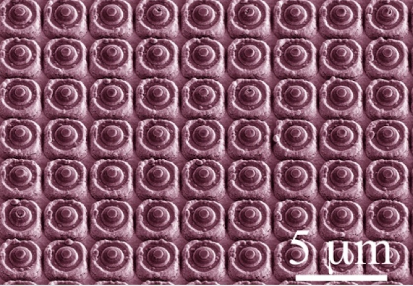
Before the wafers were diced into chips, optical elements, such as micro-lens and reflector arrays were finally fabricated on the emitters in a monolithic wafer-level scale. To achieve desired light collimation, the emitter mesa diameters were designed to be approximately a third of the pixel pitch. Therefore, for the 2.5µm pixel pitch, the emitter mesa diameter is less than a micrometer, as shown by the scanning electron microscopic image in Fig. 1 (top of page).
Fig. 2 shows an SEM image of proof-of-concept bicolour pixel array with a pitch of 40 µm (above) and optical microscopy image (below) of lit pixels in a wafer level test.
As well as pushing the boundaries of monochromatic pixel emitter dimensions, the company is also exploring polychromatic micro-display panels. These polychromatic panels were fabricated by stacking multiple sheets of blank epilayers a CMOS backplane wafer. The epilayer stacking was then followed by III-V/ compound semiconductor thin film processing sequences. Without using alignment bonding or pick-n-place, desirable pixel yield and uniformity can be achieved.
As compared to DLP and LCOS, the AMuLED display panels do not require illumination light sources. Light emission from III-V/Nitride compound semiconductors and digital image control from CMOS were integrated in a 0.5-mm-thick chip. This hybrid integration significantly reduces the complicity of the optics in VR or AR devices. Moreover, the compound semiconductor emitters deliver much higher light output intensity as compared to OLED micro emitters.
For example, JBD’s 2.5µm pixel pitch AMuLED display panels offer 1 million cd⋅m-2 at 525nm, which is several orders of magnitude higher that reported OLED micro-display performance. Furthermore, without any moving parts and containing no organic materials, the AMuLED display panels can be used in wide temperature ranges (-50degC to 100degC) and harsh environment (vibration and UV radiation) with high reliability and long life time.
Founded in 2015, JBD is currently transitioning from a research-and-development phase into a manufacturing-and-sales phase. In April 2019, JBD released a 5µm-pitch series. This series contains monochromatic panels with a resolution of 1280 by 720. The 2.5µm pitch series is scheduled to be released in late 2020. With a pilot fab established in Shanghai China, JBD continues to expand its manufacturing capacity and extend its development effort to support its customers.


