
Novel etching technique yields the smallest InGaAs FinFETs
Thermal atomic layer etching produces incredibly small InGaAs FinFETs with record-breaking performance
BY WENJIE LU, YOUNGHEE LEE, JESÚS DEL ALAMO, AND STEVEN GEORGE FROM MASSACHUSETTS INSTITUTE OF TECHNOLOGY AND UNIVERSITY OF COLORADO BOULDER
For the past five decades, the microelectronics revolution has been driven by the scaling of silicon CMOS. Reducing device dimensions has delivered continuous improvements in transistor performance, enabling this device to faithfully follow Moore’s law. The question is, how much longer can this go on?
Throughout the twentieth century, advances in CMOS technology came from shrinking the dimensions of the planar transistor. But recently the design of the device has had to change. Modifications include the introduction of three-dimensional architectures that create severe production challenges, which must be overcome when manufacturing state-of-the-art silicon multi-gate transistors, such as the latest FinFETs. This class of transistor has already reached the sub-10 nm regime – for example, the latest Intel 10 nm FinFETs feature fins that are merely 7 nm wide.
Such miniaturisation is an extraordinary feat of human engineering, unthinkable even a decade ago. And it’s not just a matter of simply reducing the width of the FinFET – this must go hand-in-hand with a fin that is tall enough to support a high current density. Do this, and you can fulfil performance criteria, but you’ll have a very fragile structure.
Another characteristic of the modern FinFET is a performance that is dominated by its surface area. So, to ensure that it work wells, it has to have a high-quality MOS interface. This requirement, which is retained as scaling continues, has to be realised with etching technologies that support sub-nanometre precision and fidelity, while yielding highly perfect interfaces. This is out of reach for today’s mainstream etching methods.
Thermal atomic layer etching
In silicon fabs, the most common method for patterning micro and nano-scale structures is plasma etching. In use since the 1970s, this essential step of CMOS fabrication has evolved, becoming ever-more sophisticated. However, it can only go so far. New forms of etching are now needed that are more benign and versatile, while providing sub-monolayer etch control, so that fabs can produce sub-10 nm, 3D structures.
Recently, a new class of etching has been attracting much attention. Known as atomic layer etching, or simply ALE, it is the most advanced etching technique today. It is essentially the reverse of atomic layer deposition (ALD), based on two self-limiting steps: the modification of the device surface by a reactive species; and then the selective etching of the modified surface, to leave an untouched substrate beneath.
ALE can be sub-divided into two types. The more common, known as plasma ALE, has realised tremendous progress in the last few years, and involves the modification of the surface by a reactive plasma, such as Cl2 plasma. Etching follows by introducing energetic ions or neutrals, such as an argon plasma, into the chamber. With this technique, etching is anisotropic – that is, directional – a useful attribute for many processes that involve pattern transfer.
The other form is thermal ALE. It avoids a plasma, instead removing material through a chemical ligand-exchange process. The reaction sequence closely resembles that of atomic layer deposition, in which pulses of chemical precursors are introduced into a reactor to complete two individual self-limiting steps. Mirroring ALD, thermal ALE is an isotropic process.
Thermal ALE is much younger than plasma ALE, having been first demonstrated in 2015, when it was used to etch an Al2O3 thin film. Since then, most reports on this technology have been limited to etching dielectric, metal and nitride thin films. There have been no device-level demonstrations.
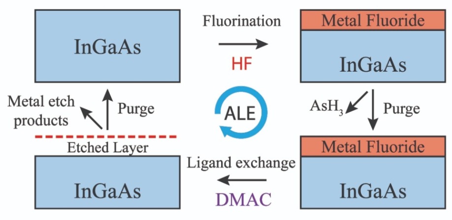
Figure 1. Schematic of a complete cycle of InGaAs thermal atomic layer etching. In the first half-cycle, the InGaAs surface is fluorinated, and metal fluorides are formed. In the second half-cycle, the metal fluorides are removed through a ligand-exchange process. The volatile etch products formed during each half-cycle are purged away.
Removing III-VsOur MIT-University of Colorado collaboration is addressing that omission, using the thermal ALE process to fabricate transistors. Efforts were initially directed at developing a thermal ALE technique for III-V compound semiconductors, and in particular InGaAs.
We have focused on this ternary, because it is a promising material for CMOS logic and RF applications. Its merits include a very high electron velocity, which is the key to achieving a high performance at a lower operating voltage than the traditional silicon MOSFETs. Recently, rapid progress is being made with this type of device, including our demonstration, in 2017, of an InGaAs FinFET with a fin width down to 7 nm.
However, until our very latest work, carried out within the last year or so, the performance of the best InGaAs FinFETs was still at some distance from its true potential, primarily due to a poor MOS interface quality.
Before we delve into the details of our work, we wish to point out that the introduction of ALD had a dramatic impact on the performance of III-V transistors. Just over ten years ago, this deposition technique made its introduction into III-V MOSFET processing. Due to its self-cleaning effect, it was instrumental in mitigating surface Fermi-level pinning at the oxide-semiconductor interface.
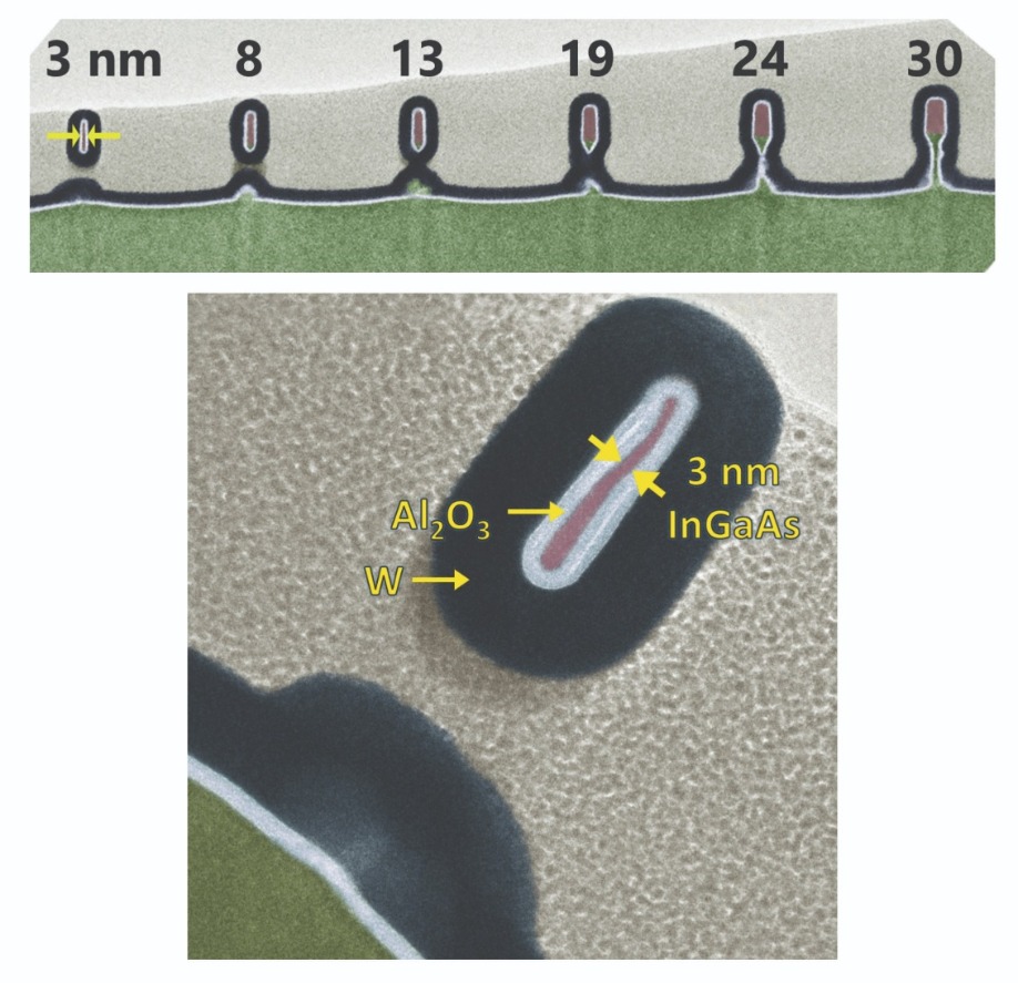
Figure 2. Cross-sectional transmission electron microscopy image of (top) InGaAs fins (fin widths of 3 nm to 30 nm) fabricated by the in situ ALE-ALD process, and (bottom) the smallest InGaAs suspended fin with a 3 nm fin width.
Since then, the performance of the InGaAs MOSFET has skyrocketed. However, issues remain. Fabricating FinFETs requires aggressive plasma etching of channel sidewalls, and this is probably to blame for compromised electron transport. We are aiming to address this with thermal ALE.After some experimentation, we have developed a working thermal ALE process for III-Vs. The first half-cycle is a surface fluorination step, using gaseous hydrofluoric acid, and the second half is a ligand-exchange process, removing metal fluorides on the surface (see Figure 1 for an outline of the sequence). By using dimethylaluminum chloride to remove the metal fluorides, we have a process that has all the etch products volatile at 300 °C, allowing them to be removed by purging. If we need to increase the depth of the etch, we simply repeat the cycle.
Trials at 300°C have determined etch rates of 0.2 Å/cycle and 0.6 Å/cycle, respectively, for InGaAs and InAlAs. In comparison, conventional self-limiting etching methods, such as digital etch, typically etch at a rate of the order of 1 nm/cycle, indicating that InGaAs thermal ALE is around fifty times slower. That’s not an issue but a blessing, as when this technology is used for deep nano-scale device fabrication, it provides unprecedented etching control and precision.
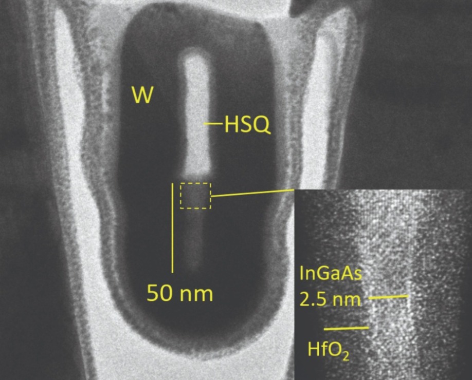
Figure 3. A cross-sectional transmission electron microscopy image of the most aggressively scaled InGaAs FinFET with fin width of 2.5 nm. Inset: close-up image of the upper portion of the fin channel.
What is even more exciting is that the similarities between ALE and ALD allow us to pair them together in the same reactor. This has enabled us to perform in situ ALE-ALD, an ideal process for forming the MOS gate stack in a FinFET. We gently etch into the fin sidewalls, in a plasma-free, isotropic fashion, using thermal ALE, before we switch to ALD to cover them with gate dielectric and metal.This approach is very promising. It completely prevents air exposure to the MOS interface, and it offers much freedom – after we have decided which precursors to introduce into the reactor, we can freely switch between etching and deposition. Due to these strengths, plus the great level of control, this process offers new ways to undertake nano-scale device fabrication that should help to significantly improve transistor performance.
To highlight the capability of twinning ALE and ALD, we have used these two technologies to fabricate a series of InGaAs-Al2O3-W gate-all-around fin structures. These devices, formed with an in situ ALE-ALD process, feature InGaAs fins with widths ranging from 30 nm down to just 3 nm (see Figure 2). We have found that when the fin width is below 20 nm, the InGaAs channel is completely suspended, due to the ALE selectivity between InGaAs and InAlAs. The in situ process also produces a remarkably sharp interface between the InGaAs and Al2O3 layers. This gave us great hope when we embarked on creating the first transistor by thermal ALE.
Miniaturised FinFETs
Using our in situ thermal ALE-ALD technique, we have fabricated InGaAs FinFETs with a fin width from 18 nm to 2.5 nm and a fin height of 50 nm (see Figure 3 for transmission electron microscopy cross-sections of these transistors). The key to making these devices, which include the most aggressively scaled III-V FinFET to date, is the extremely low etching rate of thermal ALE. Note that the FinFET features an HSQ hardmask, used for fin reactive-ion etching, that is left in the finished transistor, and a gate stack consisting of 3 nm of HfO2 and 30 nm of tungsten. The minimum gate length is 60 nm.
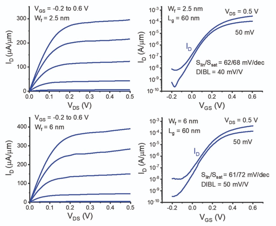
Figure 4. Output and subthreshold characteristics of InGaAs FinFETs fabricated by an in situ thermal ALE-ALD process. The FinFETs have a gate length of 60 nm, and a fin width of 2.5 nm (top row) and 6 nm (bottom row). All figures of merit are normalised by the conducting gate periphery.
The merits of in situ ALE are not limited to the fabrication of extremely small devices, but extend to significant improvements in performance that result from the lack of exposure of the critical oxide-semiconductor interface to air, as occurs in common fabrication processes. Measurements on our InGaAs FinFETs show well-behaved transistor behaviour, even for the 2.5 nm-wide fins (see Figure 4). For these transistors, in the linear and saturation regime, subthreshold swings are just 62 and 68 mV/decade, respectively. These near ideal values, highlighting the capability of these devices to sharply turn-off, stem from the high quality of the MOS interface.We have found that differences in fin width lead to changes in the maximum value for transconductance, a measure of the transistor’s turn-on behaviour. Operating at a drain-source voltage of 0.5 V, the maximum transconductance is 0.85 mS/µm for a 2.5 nm fin, and increases to 1.2 mS/µm for a device with a 6 nm fin – the latter exhibits excellent electrostatic behaviour. For all devices, off-state current is limited by gate leakage.
To evaluate the benefit of our in situ process, we have compared the characteristics of our latest FinFETs with our previous generation of InGaAs FinFETs. Both sets of transistor have the same device design, and aside from the new thermal ALE process, they are fabricated in the same way.
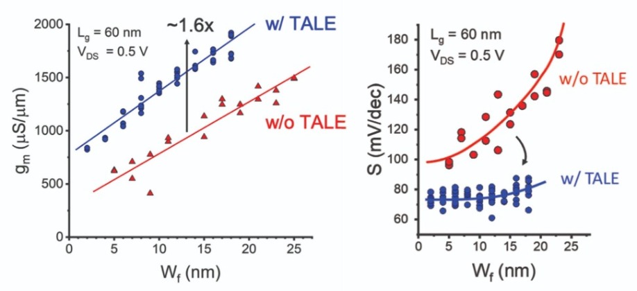
Figure 5. Scaling behaviour of (left) transconductance and (right) subthreshold swing versus fin width of InGaAs FinFETs at VDS = 0.5 V, with and without the in situ thermal ALE-ALD process. All FinFETs have a gate length of 60 nm.
Plotting the maximum transconductance and subthreshold swing as a function of fin width shows that the two types of FinFETs have a similar scaling behaviour (see Figure 5). In addition, they reveal that the thermal ALE process produces a 60 percent overall improvement in transconductance and a reduction in saturation subthreshold swing. For the new InGaAs FinFETs, the average subthreshold swings is 70 and 74 mV/dec in the linear and saturation regime, respectively. In comparison, the previous generation of devices have sub-threshold swings that are just below 100 mV for 5 nm fins, and nearly double this for 25 nm fins. This deterioration in sub-threshold swing with wider fins is minimal in devices made with the in situ ALE/ALD process.We have also observed a consistent reduction in drain-induced barrier lowering with our in situ ALE/ALD process. This finding, and the values for the maximum transconductance and subthreshold swing, underline the extraordinary enhancement in electrostatic control that results from the superior MOS interface quality obtained by the in situ thermal ALE-ALD process.
To evaluate the performance of our latest InGaAs FinFETs, we have benchmarked their peak transconductance against other state-of-the-art InGaAs FinFETs. Our survey of the literature reveals a record peak transconductance for all our III-V FinFETs with fin widths below 20 nm.
We have also compared our devices with commercial silicon FinFETs. For a 7 nm fin width, which corresponds to the 14 nm and 10 nm nodes, our InGaAs FinFETs match the performance of Intel’s 14 nm node FinFETs. This is a great result, considering our device’s lower operating voltage – VDD is 0.5 V for InGaAs and 0.7 V for silicon – and our longer gate length.
Our results are extremely encouraging, given that these transistors are the first to be made by thermal ALE. They clearly show great promise, while highlighting potential for thermal ALE, which could lead to improvements in other nano-electronic devices. This technique is truly versatile: it can be applied to a wide range of materials and device structures, such as vertical nanowires; and it offers engineers new opportunities to design and fabricate devices at the atomic level. As Feynman would say, “There’s plenty of room at the bottom!”
W. Lu et al. “First Transistor Demonstration of Thermal Atomic Layer Etching: InGaAs FinFETs with sub-5 nm Fin-width Featuring in situ ALE-ALD”, IEEE IEDM, 2018.
K. J. Kanarik ACS J. Phys. Chem. Lett. 9 481 (2018)
J. A. del Alamo Nature 479 317 (2011)


