
New approach brightens future of perovskite LEDs
Quantum confinement helps make extra bright, efficient perovskite-based LEDs
Several techniques for generation of light from electricity have been developed over the years. Devices that can emit light when an electric current is applied, are referred to as electroluminescent devices, which have become orders of magnitude more efficient than the traditional incandescent light bulb. LEDs comprise the most notable and ubiquitous category of these devices.
A myriad of different types of LED exist nowadays, which has been made possible by advances in our understanding of quantum mechanics, solid-state physics, and the use of alternative materials.
Electroluminescent devices consist of several layers, the most important being the emission layer (EML), which emits light in response to an electric current. Metal halide perovskites, with the chemical formula CsPbX3 (X = I, Br, Cl), have been recently considered as promising materials for fabricating the EML. However, current perovskite-based LEDs (PeLEDs) perform poorly compared with organic LEDs, which are typically used to design displays of TVs and smartphones.
Several researchers have suggested fabricating PeLEDs using low-dimensional (i.e., emitting structural units are connected on a plane or linearly in the crystal structure) perovskites that offer improved light-emission performance based on the quantum confinement effect of excitons. An exciton is an electron-hole pair that emits photon efficiently. However, using low-dimensional perovskites has an intrinsic drawback in that the conducting properties, i.e. low mobility, of these materials are very poor, and this lack of low mobility leads to low power efficiency.
Interestingly, as discovered by a team of researchers led by Hideo Hosono from the Tokyo Institute of Technology, it is possible to design highly efficient PeLEDs using three-dimensional (3D) perovskites, which have superior mobility of electron and hole and hence would address the limitation of low-dimensional perovskites.
The team investigated if the quantum confinement effect that occurs in low-dimensional materials using new electron transport layer adjacent to the perovskite and results in attractive light-emission properties, could be achieved in 3D materials. In an electroluminescent device, the EML is sandwiched between two layers: the electron transport and hole transport layers. These two layers play a key role in ensuring good conducting properties of the device. The team found that the energy-level characteristics of these layers also play a crucial role in emission efficiency of the EL.
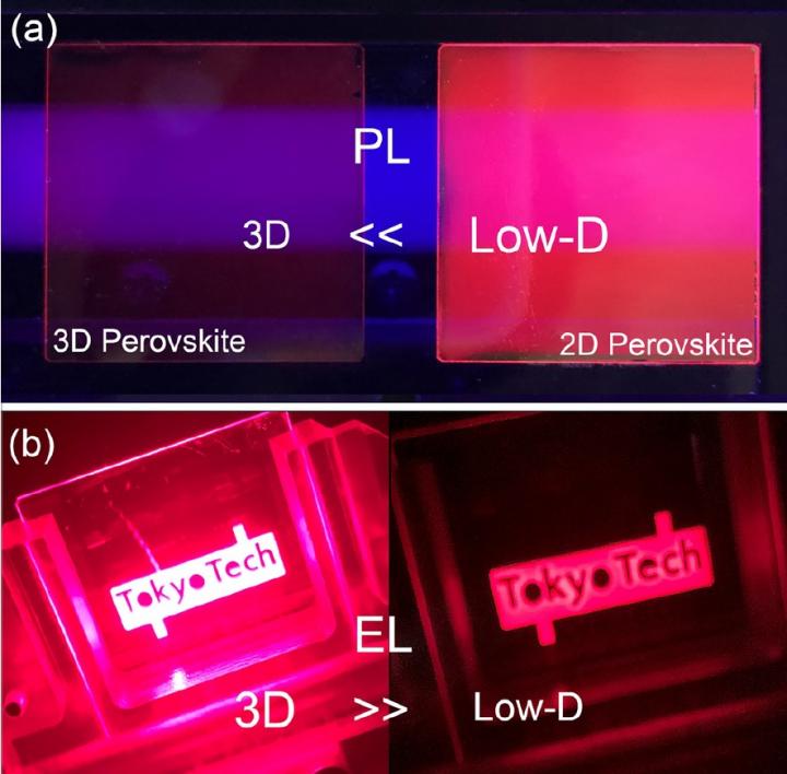
By tuning the characteristics of the electron and hole transport layers in PeLEDs, the team could prevent the above effect by ensuring that excitons remain confined in the emission layer. "The whole device structure can be regarded as a scaled-up low-dimensional material in a sense if the energy levels of the electron/hole transport layers are sufficient for exciton confinement," explains Hosono. The team reported 3D PeLEDs with record-setting performance in terms of high brightness and power efficiency and low operating voltage. Figure 1 shows a comparison between low-dimensional and 3D perovskite-based luminescent devices.
Aside from these tangible practical achievements, this research sheds light into how the exciton-related properties of a material can be influenced by the adjacent layers and provides a strategy that can be readily exploited in the development of optical devices. "We believe this study provides new insight into the realization of practical PeLEDs," concludes Hosono. With such interesting advances in light-emitting materials, it seems that a (literally) brighter future awaits.
The picture above shows: (A) photoluminescence and (B) electroluminsecence in low-dimensional and 3D perovskite-based devices. Although low-dimensional perovskite exhibits better PL properties than 3D perovskite, the latter has better EL properties, which can be exploited to design very bright and efficient PeLEDs.


