
Ascatron eyes mass markets
With its latest funds, Ascatron is ready to scale production of high voltage SiC devices to meet growing market demands, reports Rebecca Pool.
In July, this year, Sweden-based SiC power semiconductor developer, Ascatron, revealed it had raised €3.5 million in funds, following the sale of shares in Basic Semiconductor, a joint venture business in China.
Now focusing on product development and volume production, the company is currently providing its first devices - 1200V and 1700V diodes - to customers for design-in projects, with MOSFETs scheduled for volume production next year.
“Right now we are working on 1200V devices and higher,” says Ascatron chief executive, Christian Vieider. “We see our competitors having difficulties getting out products with higher voltages than 1700V so high voltage devices are our focus.”
“Our next step is to increase capacity, and we will coordinate this in line with customer demand,” he adds. “We have good connections with suppliers of epitaxy equipment and we see this as being feasible within a one-year time period.”
Critical technology
Ascatron span out of Swedish research institute, Acreo, in 2011 and has since developed myriad processes for manufacturing SiC semiconductors including substrate buffers, SiC epitaxy, deep trench etching and more.
At the heart of its processes lies the company's proprietary technology, '3DSiC', that is based on embedded epitaxial growth methods that replace the conventional process of doping with ion implantation during fabrication.
Doped material is grown over 3D structures, such as trenches and doped patterns, reducing electric fields at Schottky contacts and MOS interfaces and boosting device performance. For example, Ascatron claims losses can be reduced by up to 30% compared to devices fabricated via conventional processes.
Crucially, the company has spent the past year transferring the process from its in-house clean room at the Electrum Laboratory, just outside Stockholm, to an external foundry. According to Vieider, Ascatron's design is now cost-compatible with competitors, and the company is now gearing up for volume production.
“We use this buried grid in our design to shield off electric fields and then fabricate the Schottky diode or MOSFET on top of this,” says Vieider. “This was a new process step for the foundry but we've got this to work and we are now getting the same results at the foundry as in our own clean room, which is a big achievement for us.”

Ascatron chief executive, Christian Vieider.
Up until now, Ascatron has been manufacturing some 1000 epi-wafers a year on its own equipment but Vieider is keen to triple production in the short term, and take volumes to at least 1000 a month in the next three to four years. As he points out, the foundry capacity is more than 20,000 wafers a year, although, in his words: “It could take some time for us to get to this level [of production] from where we are now.”
And as a handful of SiC device makers have been making the tricky transition from 100mm to 150 mm, grappling with yields and defect levels, Vieider anticipates Ascatron production will be centred on the 150 mm wafer size for the foreseeable future. “Six inch wafers are still not as high quality as four inch wafers so in terms of quality we would be stepping back a couple of years by shifting to eight inch wafers, even if these were available to buy,” he says.
But could industry issues over SiC wafer supply stymie Ascatron's plans for volume production? Vieider isn't worried.
“Everyone is fighting these wafer shortages but we haven't seen any problems yet,” he says. “For us volume production starts at 1000 wafers a month and from what we understand these volumes are available.”
“Also, if we talk about scaling over a two year period, our suppliers don't anticipate this being a problem as they are investing heavily in capacity,” he adds.
So what now for Ascatron? With its fabrication process qualified, the company is working on product qualification, which Vieider reckons will be achieved towards the end of 2020. The company is targeting high power, high voltage applications, including industrial and the all-important electric vehicles, and its focus will remain firmly here.
“We have seen interest in 650V devices but right now we need to focus on our buried grid technology and there is a clear advantage for this at the higher voltages,” says Vieider. “Also, it's important for us to be competitive with other silicon carbide vendors by having a design where we can increase the current density and make our chips smaller, so we can get more chips on every wafer.”
And importantly, Vieider is confident that Ascatron is ready to compete with the likes of Infineon and Cree. “From customer feedback, Infineon is the reference, so we have been evaluating our first products against its high-performing devices,” he says. “We have our innovative design which gives us many advantages compared to these bigger companies.”
At the same time, Ascatron can also tailor its diode design to customer requirements. “Until recently, we were considering packaging but we've now reduced our product offering to bare dies so that our customers take care of the packaging and offer a complete module,” he says. “In this way Infineon could also be our customer.”
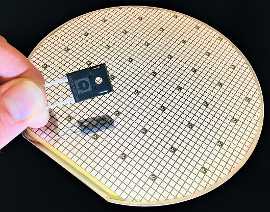
Main image: A 150mm device wafer with 1700V/20A 3DSiC diode chips from Ascatron.


